Video Lecture
Theory For Making Notes
Developments in the semiconductor field were rapid after 1945 and by 1949, the theory of p-n junctions had been established. At this time, theory of a junction transistor was given by Shockley .
The junction transistor is composed of an npn or pnp sandwich. An npn transistor consists of a p type semiconductor sandwiched between two layers of n type semiconductors. Whereas a pnp transistor consists of a n type semiconductor sandwiched between two layers of p type semiconductor. Hence a transistor consists of three regions namely emitter , base and collector and hence it is also called a triode. The emitter region is made of a semiconductor which is highly doped. The base region is kept thin and made of a semiconductor which is lightly doped and the collector region is the largest of all the three regions.
Symbols of transistors

There are three parts of a transistor which are as follows:
(i) Emitter: Emitter can be defined as the region from which charge carriers are injected into the base.
(ii) Collector: That electrode which collects the above majority carriers.
(iii) Base: It provides junctions for proper interactions between the emitter and the collector.
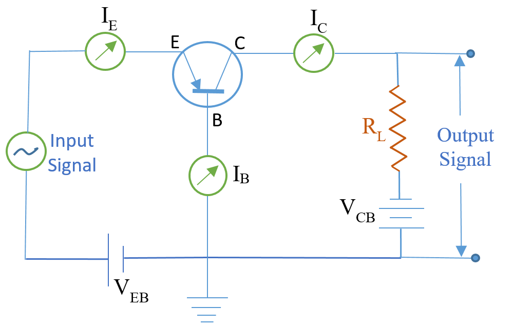
Working of a transistor in Common Emitter mode
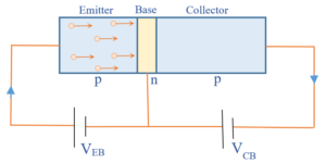
The positive terminal of the battery \displaystyle {{V}_{{EB}}}repels the holes in the left p region. Under the action of this repulsion these holes enter into the base region which is n type. The base region is very thin and lightly doped, so that the number of free electrons in the base region is very small ,due to this 95 to 98% of the holes coming from the emitter are able to pass through the base region. Whereas 2 to 5% of the holes are destroyed in the base as a result of recombination with free electrons. This recombination of the holes with the electrons in the base region makes the base current Ib. The remaining holes which are able to pass through the bases enter the collector region and are attracted towards the –ve terminal of the battery \displaystyle {{V}_{{CB}}} . As one hole comes in contact with the terminal an electron emitted by the terminal enter into it and destroy it. This process forms the collector current. For each recombination of the electron and holes in the base and collector region, an electron leaves the covalent bonding near the +ve terminal of the battery \displaystyle {{V}_{{EB}}}. And enter into the terminal, which causes the emitter current to flow. Hence the emitter current is equal to the sum of the base current and the collector current. This shows that the current inside the transistor is carried by the holes whereas outside, the electrons carry it. If \displaystyle {{I}_{{B}}} is the base current , \displaystyle {{I}_{{C}}} is the collector current & \displaystyle {{I}_{{E}}} is the emitter current then
\displaystyle {{I}_{E}}=\text{ }{{I}_{B}}+\text{ }{{I}_{C}} also from the above discussion we can conclude that \displaystyle {{I}_{C}}>>\text{ }{{I}_{B}}. This fact is used in the amplifier circuit made of a transistor.
TRANSISTOR AS AN AMPLIFIER
Amplifier
It is a device which increases the strength of an electric signal by drawing energy from a separate source and supplying it to the signal.
Common base amplifier
A npn transistor is shown in the diagram given below in common base mode. The input signals are fed into emitter-base circuit. Output signals are taken from collector-base circuit. High load resistance ( \displaystyle {{R}_{L}}) is connected between collector and base. Input circuit is forward biased while the output circuit is reverse biased. Hence input circuit may be considered as a low resistance circuit and the output circuit may be considered as a high resistance circuit. So the introduction of a high resistance \displaystyle {{R}_{L}} in the output circuit is not going to affect the characteristics of the transistor. This property, however, enables us to amplify.

The connections for a pnp common base amplifier are exactly as above except that the polarities of the batteries are reversed and the transistor used in a pnp transistor in place of npn transistor.
Due to the imposition of signal, voltage of emitter base circuit undergoes a variation which in turn results in collector current, \displaystyle {{I}_{C}} . Since \displaystyle {{R}_{L}} is very high, variation in \displaystyle {{I}_{C}} produces a large variation in voltage across it, thus amplifying the input signal.
Various Parameters Of a Common Base Amplifier
1. The ac Voltage Gain (AV)
Let \displaystyle \delta {{I}_{E}} = small change in \displaystyle {{I}_{E}}
\displaystyle \delta {{I}_{C}} = small change in \displaystyle {{I}_{c}}
\displaystyle {{E}_{i}} = input voltage
\displaystyle {{R}_{i}} = input resistance
\displaystyle {{R}_{L}} = load resistance
\displaystyle {{E}_{o}} = output voltage
Here \displaystyle {{E}_{i}}={{R}_{i}}\times \delta {{I}_{E}} …(i)
and \displaystyle {{E}_{0}}={{R}_{L}}\times \delta {{I}_{C}} …(ii)
voltage gain {{A}_{v}} =\frac{{{{E}_{0}}}}{{{{E}_{i}}}}=\frac{{{{R}_{L}}\delta \,{{I}_{C}}}}{{{{R}_{i}}\delta \,{{I}_{E}}}}
hence {{A}_{v}} ={{\alpha }_{{ac}}}\times \frac{{{{R}_{L}}}}{{{{R}_{i}}}}\ \left[ {\because \frac{{\delta \,{{I}_{C}}}}{{\delta \,{{I}_{E}}}}=\alpha } \right]
here \frac{{R}_{L}}{{R}_{i}} is called Resistance gain
therefore {{A}_{v}} ={{\alpha}_{ac}}\times{Resistance{ } gain}.
2. The ac Current Gain ( \displaystyle {{\alpha }_{{ac}}})
As written above, ratio of change in collector current ( \displaystyle \delta {{I}_{C}}) and change in emitter current. ( \displaystyle \delta {{I}_{E}}) at constant collector voltage ( \displaystyle \delta {{V}_{C}}) is called current gain.
Hence Current gain {{\alpha}_{ac}} =\frac{{\delta {{I}_{C}}}}{{\delta {{I}_{E}}}}, at constant VC.
Note: dc current gain \displaystyle \alpha was simply ( \displaystyle {{I}_{C}}/{{I}_{E}}) i.e. without \displaystyle \delta.
3. Power Gain
Small Change in power output = \displaystyle {{E}_{0}}\times \delta {{I}_{C}}
Small Change in power input = \displaystyle {{E}_{i}}\times \delta {{I}_{E}}
Therefore power gain =\frac{{{{E}_{0}}\times \delta {{I}_{C}}}}{{{{E}_{i}}\times \delta {{I}_{E}}}}
\displaystyle \Rightarrow power gain =\frac{{({{R}_{L}}\times \delta {{I}_{C}})\times \delta {{I}_{C}}}}{{({{R}_{i}}\times \delta {{I}_{E}})\times \delta {{I}_{E}}}}
\displaystyle \Rightarrow power gain ={{\left( {\frac{{\delta {{I}_{C}}}}{{\delta {{I}_{E}}}}} \right)}^{2}}\times \frac{{{{R}_{L}}}}{{{{R}_{i}}}}.
Finally power gain =\text{ }\alpha _{{\mathbf{ac}}}^{\mathbf{2}}\times \text{Resistance gain}.
Common emitter amplifier
Common emitter amplifier is used as a voltage amplifier. The connections for a pnp common emitter amplifier are exactly the same except the polarities of the batteries are reversed.

(NPN) Common Emitter Amplifier (Fig-a)

(PNP) Common Emitter Amplifier (Fig-b)
Take special notices that the phase difference between input and output signals is 180°.
The input signal (to be amplified) is connected in the emitter base circuit and output signal is taken from the collector-emitter circuit. Imposition of signal results in the variation of base current \displaystyle {{I}_{B}} and hence a variation in \displaystyle {{I}_{C}}. This produces a large variation in the voltage across \displaystyle {{R}_{L}} thus causing amplification.
Various Parameters Of a Common Emitter Amplifier
Current Gains
Current gain is also called common-emitter current amplification factor. Which may be of two types
1. dc current gain ( \displaystyle \beta )
2. ac current gain ( \displaystyle {{\beta}_{ac}} )
dc Current Gain ( \displaystyle \beta )
It is defined as the ratio of the collector current ( \displaystyle {{I}_{C}}) and the base current ( \displaystyle {{I}_{B}})
hence \beta =\frac{{{{I}_{C}}}}{{{{I}_{B}}}}=\frac{{{{I}_{C}}}}{{{{I}_{E}}-{{I}_{C}}}}
dividing each term by {{I}_{E}}
\displaystyle \Rightarrow \beta=\frac{{{{I}_{C}}/{{I}_{E}}}}{{1-{{I}_{C}}/{{I}_{E}}}}
\displaystyle \Rightarrow \beta=\frac{\alpha }{{1-\alpha }} [\because \ \alpha ={{I}_{C}}/{{I}_{E}}]
While \displaystyle \alpha is always less than 1 (generally 0.98 or less), the value of \displaystyle \beta is always higher than 1.
If \alpha =0.9, { } \beta =\frac{{0.9}}{{1-0.9}}=9
If \alpha =0.95,\ \beta =\frac{{0.95}}{{1-0.95}}=19
If \alpha =0.98,\ \beta =\frac{{0.98}}{{1-0.98}}=49
Hence, slight variation in \alpha cause large variation in \displaystyle \beta .
ac Current Gain ( \displaystyle {{\beta}_{ac}} )
It is defined as the ratio of the small change in the collector current ( \displaystyle \delta {{I}_{C}}) and the corresponding small change in the base current ( \displaystyle \delta {{I}_{B}}) at constant collector voltage
hence {{{\beta }_{{ac}}}=\frac{{\delta {{I}_{C}}}}{{\delta {{I}_{B}}}},\ \text{at constant }{{V}_{C}}}
It’s value lies between 15 and 50 generally for a transistor.
Voltage Gain
Voltage input = \displaystyle \delta {{I}_{B}}\times {{R}_{i}}
Voltage output = \displaystyle \delta {{I}_{C}}\times {{R}_{L}}
Hence Voltage Gain =\frac{{\delta {{I}_{C}}\times {{R}_{L}}}}{{\delta {{I}_{B}}\times {{R}_{i}}}}
{\text{Voltage gain }=\text{ }{{\beta }_{{\text{ac}}}}\text{ }\times \text{ Resistance gain}}.
Power gain
Power output = \displaystyle {{E}_{0}}\times \delta {{I}_{C}}
Power input = \displaystyle {{E}_{i}}\times \delta {{I}_{B}}
Hence Power{ } gain =\frac{{{{E}_{0}}\times \delta {{I}_{C}}}}{{{{E}_{i}}\times \delta {{I}_{B}}}}
\displaystyle \Rightarrow { }Power{ } gain =\frac{{({{R}_{L}}\times \delta {{I}_{C}})\times \delta {{I}_{C}}}}{{({{R}_{i}}\times \delta {{I}_{B}})\times \delta {{I}_{B}}}}
\displaystyle \Rightarrow { }Power{ } gain={{\left( {\frac{{\delta I}}{{\delta {{I}_{B}}}}} \right)}^{2}}\times \frac{{{{R}_{L}}}}{{{{R}_{i}}}}
{\text{Power{ } gain }=\text{ }\beta _{{\text{ac}}}^{\text{2}}\times \text{Resistance gain}} .
Phase difference in input and output voltages (phase relationship) in case of common emitter amplifier
\displaystyle {{V}_{{CE}}}={{V}_{{CC}}}-{{I}_{C}}{{R}_{L}}
[from the circuit diagram drawn for common emitter amplifier vide figure (a).
When positive half of an ac voltage comes from input signal, it adds to the forward biasing. This increase emitter current ( \displaystyle {{I}_{E}}). This increase collector current ( \displaystyle {{I}_{C}}). This decreases \displaystyle {{V}_{CE}} [from above given relationship]. Hence as positive signal voltage increases, \displaystyle {{V}_{CE}} voltage decreases and vice-versa.
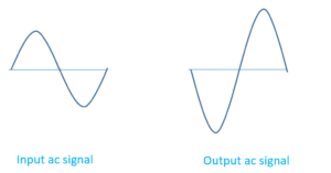
Due to this, the input signal voltage & output voltage both are out of phase by \displaystyle {{180}^{o}}.
Illustration
In a silicon transistor, base current is changed by 30 \displaystyle \mu A. This results in a change of 3 mA in the collector current.
(a) Find the input resistance, ac current gain ( \displaystyle {{\beta}_{ac}} ) of transistor.
(b) The transistor is used as an amplifier with the load resistance 5 kW. What is the voltage gain of the amplifier?
Solution
(a)
\delta {{I}_{b}}=30\mu \text{A}
\delta {{V}_{b}}=0.03\text{V}\text{.}
\delta {{I}_{e}}=3\text{mA}
Input resistance, {{R}_{1}}=\frac{{\delta {{V}_{b}}}}{{\delta {{I}_{b}}}}=\frac{{0.03}}{{30}}\times {{10}^{{-6}}}=1000\,\text{ohm}
Current gain of the transistor =\frac{{\delta {{I}_{c}}}}{{\delta {{I}_{b}}}}
=\frac{{3\times {{{10}}^{{-3}}}}}{{30\times {{{10}}^{{-6}}}}}
=100
(b)
Voltage gain of the amplifier = current gain × resistance gain
=\frac{{\text{100}\times \text{output}\ \text{resistance}}}{{\text{input}\ \text{resistance}}}
=\frac{{100\times 5000}}{{1000}}=500.
Illustration
The input resistance of transistor in common-emitter configuration is \displaystyle {{R}_{i}}=\text{ }\mathbf{2}.\mathbf{5}\Omega and load resistance is, \displaystyle {{R}_{L}}=\text{ }5.6k \Omega If the current gain is \displaystyle \beta = 90 and applied voltage is, VI = 13 mV, calculate the resistance gain, voltage gain and the value of the output signal.
Solution
(a)
Resistance gain =\frac{{{{R}_{L}}}}{{{{R}_{i}}}}=\frac{{5.6}}{{2.5}}=2.24
(b)
Voltage gain = current gain × resistance
\text{gain}=\beta \left( {\frac{{{{R}_{L}}}}{{{{R}_{i}}}}} \right)=90\times 2.24=201.6
(c)
Output voltage = voltage gain × input voltage
= \displaystyle 201.6\times 13\times {{10}^{{3}}}
= 2620.8 mV.
TRANSISTOR AS AN OSCILLATOR
“It is a device that generates an ac signal of known frequency from a dc input”. If the output voltage or current has the form of sine wave w.r.t. time, the device is called oscillator.
(To produce undamped electromagnetic oscillations)

L` = High impedance coil
L = Low impedance coil
C = Variable capacitor connected in parallel with L, to give required frequency of oscillations. When key K is pressed, a small collector current flows through L`. This transient (i.e. during the time when the current is building up to take up its final magnitude) current in L` induces a small voltage in L. This small voltage produces a small current in emitter base circuit.
(The emf in the base-emitter circuit is provided by this induced emf in L).
Important point to note
L` and L connected in two ways. First, they are wound over each other and thus linked with each other externally. If current rises or falls in L`, it will induce a corresponding emf in L. Secondly, they are connected through the transistor. L` is in collector-base circuit and L is in emitter-base circuit.
Now what actually happens in when key K is closed, current starts building up in L`. This induced emf is L provides this necessary voltage in the emitter-base circuit, thus producing emitter current \displaystyle {{I}_{E}}. If this induced emf in L produced forward biasing in emitter-base circuit, this thus produced \displaystyle {{I}_{E}} further increases \displaystyle {{I}_{C}} through the transistor, because \displaystyle {{I}_{E}}=\text{ }{{I}_{B}}+\text{ }{{I}_{C}}. This is called feed back system.
This cycle repeats till \displaystyle {{I}_{C}} reaches some saturation level overshooting its otherwise steady value which it should have had in the absence of mutual inductance between L` and L.
When this saturation limit reaches, increasing process in \displaystyle {{I}_{C}} stops. Hence, the rate of changing of flux linked in L also stops. This results in the reduction of induced emf in L to zero (as per Faraday’s law of EMI).
Thereafter, thus \displaystyle {{I}_{C}} starts decreasing, to try to attain its otherwise steady-state value i.e. to minimize its overshoot value. As soon as, this stars happening, this starts inducting emf in L in the opposite direction while causes \displaystyle {{I}_{C}} to overshoot its otherwise steady state value to be but in the opposite direction.
This thus causes oscillations in the value of \displaystyle {{I}_{C}} as well as in \displaystyle {{I}_{E}}.
A variable capacity capacitance is introduced in parallel with L` as shown. This values of L and C can be so chosen as to produce oscillations of the required frequency as per the following formula.
{f=\frac{1}{{2\pi \sqrt{{LC}}}}} .
Characteristics of a transistor in common emitter mode
- Input characteristic
- Output characteristic
- Transfer characteristic
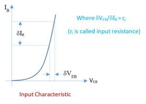
Input Characteristic
This is a graph drawn between \displaystyle {{I}_{B}} and \displaystyle {{V}_{b}} at constant \displaystyle {{V}_{C}}. This graph is similar to that of the forward biased p-n junction diode. This shows that initially the base current increases slowly with rise in the base potential till the base potential is less than the potential barrier. As soon as the base potential is made more than the potential barrier the current increases rapidly, which shows that the resistance of the first junction of the transistor called input resistance is very small.
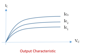
Output characteristic
This is the graph drawn between \displaystyle {{I}_{C}} and Vc at constant \displaystyle {{I}_{B}}. This graph shows that initially there is sharp rise in the collector current with rise in the collector potential but after initial rise the collector current becomes constant and independent of the collector potential. After this it is found that the collector current does not increases with increase in collector potential. If this saturated collector current has to be increased further then we have to increase the input base current. Hence we conclude that after saturation the collector current is controlled by the base current.
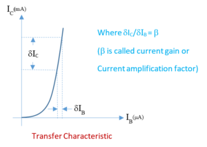
Transfer characteristic
It is the graph drawn between the base current and the collector current while \displaystyle {{V}_{C}} is kept constant. This graph shows that for a small increase in the base current there is a large increase in the collector current. This happens due to the fact that the base region is very thin and lightly doped due to which 95 to 98% of the current carriers coming from the emitter are able to pass through it without recombination with opposite charges. Hence the base current is formed due to 5% recombination of hole and electrons in the base region whereas the collector current is formed due to 95 to 98% of the current carriers reached in it without recombination in the base
region. As a result if the base current is changed by a small amount the corresponding change in the collector current is very large. The ratio of the change in collector current and the change in the base current is called current gain or current amplification factor denoted by \displaystyle \beta . Hence \displaystyle \beta =\frac{{{{I}_{C}}}}{{{{I}_{B}}}}
Derivation Of Voltage gain in a Common Emitter Amplifier
In order to use a transistor as an amplifier the emitter base junction is forward biased and the base collector junction is reverse biased. In a common emitter amplifier , the load is connected between the collector and the and the dc supply. An ac input signal Vs is superimposed on the bias Vbe as shown in figure.
As the ac signal varies it changes the base voltage \displaystyle {{V}_{{BE}}} which in turns changes the input base current \displaystyle {{I}_{{B}}}. this variation of the base voltage and base current can be represented on the input characteristic of the transistor as shown in the graph. During +ve half cycle of the input signals it makes the first p-n junction forward biased and during the negative half cycle it makes the first p-n junction reverse biased. Due to this during +ve half cycle the total forward biasing voltage across the base-emitter junction becomes \displaystyle {{V}_{{BB}}}+{{V}_{s}} , and during –ve half cycle it becomes \displaystyle {{V}_{{BB}}}-{{V}_{s}}. As a result the base current changes from \displaystyle {{I}_{{{{B}_{1}}}}} to \displaystyle {{I}_{{{{B}_{2}}}}} during the +ve and –ve half cycle of the applied ac signals.
Applying Kirchoff’s loop rule in the input circuit we get
\displaystyle {{V}_{{BE}}}=\text{ }{{V}_{{BB}}}+\text{ }{{V}_{S}} —– (1)
Differentiating the above equation we get
\displaystyle \delta {{V}_{{BE}}}=\delta {{V}_{S}} —– (2)
Hence due to application of the ac signal \displaystyle {{V}_{S}} the base potential \displaystyle {{V}_{BE}} changes by \displaystyle \delta {{V}_{{BE}}} which is equal to \displaystyle \delta {{V}_{{S}}} i.e. change in the ac voltage applied.
As the base region is very small and lightly doped as compared to the collector region therefore a small change in the base current produces a large variation in the collector current. This variation of the base current and the corresponding collector current can be shown on the transfer characteristic. From the graph it can be observed that the amplitude of the output wave i.e. collector current wave is very large as compared to the amplitude of the input ac signal which produces base current wave. The ratio of the amplitude of the collector current and the amplitude of the base current wave is called current amplification factor or current gain denoted by \displaystyle \beta .
Hence \displaystyle \beta =\frac{{\delta {{I}_{C}}}}{{\delta {{I}_{B}}}}. This value is always be more than 1 and hence the output signals are always be an amplified form of the input signals due to which this circuit is called an amplifier.
Voltage gain ( \displaystyle {{A}_{V}}) of the amplifier:
The voltage gain is defined as the ratio of the variation of the output voltage i.e. \displaystyle \delta {{V}_{o}} and the variation of the input signal voltage i.e. \displaystyle \delta {{V}_{S}} . hence
\displaystyle {{A}_{V}}=\frac{{\delta {{V}_{o}}}}{{\delta {{V}_{S}}}} —– (3)
From equation no (2) put the value of \displaystyle \delta {{V}_{S}} in equation no (3) we get
\displaystyle {{A}_{V}}=\frac{{\delta {{V}_{o}}}}{{\delta {{V}_{{BE}}}}}~ —– (4)
Applying Kirchoff’s loop rule in the output circuit of the amplifier we get
\displaystyle {{V}_{{CC}}}\text{ }=\text{ }{{V}_{{RL}}}+\text{ }{{V}_{O}}
On differentiating the above equation we get
\displaystyle 0=\delta {{V}_{{RL}}}+\delta {{V}_{o}}
OR \displaystyle \delta {{V}_{o}}=-\delta {{V}_{{RL}}} —– (5)
From equation no(5) put the value of \displaystyle {\delta {{V}_{o}}} in equation no (4) we get
\displaystyle {{A}_{V}}=\frac{{\delta {{V}_{RL}}}}{{\delta {{V}_{{BE}}}}}. —– (6)
Substituting \displaystyle \delta {{V}_{{RL}}}={{R}_{L}}\times \delta {{I}_{C}} and \displaystyle \delta {{V}_{{BE}}}={{r}_{i}}\times \delta {{I}_{B}} in the equation no. (6) we get
\displaystyle {{A}_{V}}=-\frac{{{{R}_{L}}\times \delta {{I}_{C}}}}{{{{r}_{i}}\times \delta {{I}_{B}}}}
\displaystyle {{A}_{V}}=-\beta \frac{{{{R}_{L}}}}{{{{r}_{i}}}} —– (7)
Transconductance
It is defined as the ratio of the \displaystyle \delta{{I}_{C}} and \displaystyle \delta{{V}_{BE}} of a transistor in common emitter circuit. It is denoted by \displaystyle {{g}_{m}}.
Hence \displaystyle {{g}_{m}}~=\frac{{\delta {{I}_{C}}}}{{\delta {{V}_{{BE}}}}}
Putting \displaystyle {{V}_{{BE}}}={{r}_{i}}\times \delta {{I}_{B}} in the above equation we get
\displaystyle {{g}_{m}}~=\frac{{\delta {{I}_{C}}}}{{\delta {{I}_{B}} \times {{r}_{i}}}}
\displaystyle {{g}_{m}}~=\frac{\beta }{{{{r}_{i}}}}
putting this value of \displaystyle {{g}_{m}} in the equation (7) we finally get
\displaystyle {{A}_{V}}=-{{g}_{m}}.{{R}_{L}}
The negative sign of the voltage gain signifies that the amplified output wave of ac signals has a phase difference of \displaystyle {{A}_{V}}=-{{g}_{m}}.{{R}_{L}} radians with the input ac signals.
Saturation state of a transistor
From the final expression of \displaystyle {{A}_{V}} we find that by increasing \displaystyle {{R}_{L}} we can increase the \displaystyle {{A}_{V}} to any desired high value, but this is not the fact. As our output voltage \displaystyle {{V}_{O}} is nothing but \displaystyle {{V}_{CE}} hence on applying Kirchoff’s law in the output circuit of the transistor we get
\displaystyle {{V}_{{CC}}}={{V}_{{RL}}}+\text{ }{{V}_{O}}
\displaystyle \Rightarrow { } \displaystyle {{V}_{{CC}}}\text{ }=\text{ }{{I}_{C}}.{{R}_{L}}\text{ }+\text{ }{{V}_{{CE}}}
\displaystyle \Rightarrow { }{{V}_{{CE}}}\text{ }=\text{ }{{V}_{{CC}}}-\text{ }{{I}_{C}}.{{R}_{L}}\text{ }
From the above equation we find that if the value of \displaystyle {{I}_{C}}.{{R}_{L}} is increased , \displaystyle {{V}_{{CE}}} will decrease and if it will become less than \displaystyle {{V}_{{BE}}} then the second p-n junction between the base and collector will also become forward biased and the amplification will stop. Because for amplification it is necessary that the first p-n junction should be forward biased and the second p-n junction is reversed biased. Hence beyond a certain high value of \displaystyle {{I}_{C}}.{{R}_{L}} amplification is not possible and therefore the transistor is said to be saturated.
Cut-off state of transistor
As we know that the applied ac signals increases and decreases the base-emitter potential Vbe. During positive half cycle the forward biasing voltage for base-emitter junction i.e. Vbe becomes \displaystyle {{V}_{{BB}}}+\text{ }{{V}_{S}}, and during negative half cycle the forward biasing voltage for base-emitter junction becomes \displaystyle {{V}_{{BB}}}-\text{ }{{V}_{S}}. this means that if the peak value of ac signals is more than \displaystyle {{V}_{{BB}}} then during negative half cycle the biasing voltage of base-emitter junction will become negative i.e. the base-emitter junction will become reverse biased. Due to which the transistor will not work during negative half cycle of the ac signals. This is called cut-off state of the transistor.
LOGIC GATES
NOT Gate
A NOT gate has only one input (A) and one output (Denoted by B or Y). The logic symbol and truth table are given in the figure.The output of the NOT gate is opposite to its input due to which it is also called an inverter gate. This relation between output and input can be written in the form of an equation \displaystyle \text{Y}=\overset{{\_\_}}{\mathop{\text{A}}}\,. This equation is termed as Boolean expression of NOT gate. This expression should be read as that Output Y is a compliment (opposite) of input A. Therefore we find that when the input is 1 the output is 0 and vice versa.

A NOT gate can not be realised by the diode and we have to use a transistor. A simple circuit to realise a NOT gate is shown in figure .It is a common emitter circuit with aresistance {{R}_{b}} connected with the base and a resistance {{R}_{C}} connected to the collector. The emitter is given zero potential by earthing (Understood as it is a common emitter circuit) .
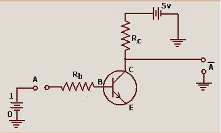
The input of the circuit is the left end of the resistance {{R}_{b}}. The output is taken as collector potential {{V}_{C}} and is where \displaystyle \overset{{\_\_}}{\mathop{\text{A}}}\, is wriiten in the circuit. From the output circuit it is clear that
\displaystyle {{V}_{C}}+{{I}_{C}}{{R}_{C}}=5
or \displaystyle {{V}_{C}}=5-{{I}_{C}}{{R}_{C}} —(1)
Now working of NOT gate can be explained using equation (1)
Working
When the left end of the resistance {{R}_{b}} i.e. input is connected to 0 potential the collector-base is reverse biased and the base emitter junction is also not forward biased. Therefore the base current is 0, hence the collector current is zero. From equation (1) If {{I}_{C}} is zero the output collector potential {{V}_{C}} is equal to 5 which is maximum and denoted by 1. So we found that when the input is 0 the otput is 1
When the left end of the resistance {{R}_{b}} i.e. input is connected to 1 the base emitter junction is forward biased and hence a finite base current flows in the circuit. Due to which a corresponding large collector current flows in the output circuit. From equation 1 we find that as {{I}_{C}} is large the output {{V}_{C}} becomes minimum and is devoted by 0. Hence we find that when input is 1 the output is 0.
Hence the truth table is satisfied.
We find that the circuit can perform the function of a NOT gate
AND Gate
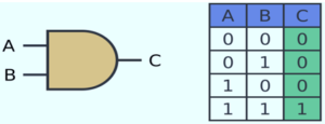
It has two inputs (A and B)and one output ( May be denoted by C or Y). The logic symbol and the truth table of an AND gate are given in the figure. As the output is C = A.B therefore in the AND gate we find that the output will be maximum i.e. 1 only when all the inputs of the gate are maximum i.e. 1.
The circuit using pn junction diodes by which the AND gate can be realised is given in figure The resistor R is connected to the positive terminal of a 5v battery permanently as shown in the figure. The N region of two Diodes {{D}_{1}},{{D}_{2}} servs as input A and B of the AND gate circuit. The potentaial at Y is taken as output. Let the output potential at Y is devoted by {{V}_{o}}. From the output circuit {{V}_{o}} can be calculated using KVL.
\displaystyle {{V}_{R}}+\text{ }{{V}_{O}}=5
or \displaystyle {{V}_{O}}=5-{{V}_{R}}
or \displaystyle {{V}_{O}}=5-I.R —(2)
Now working of the circuit can be explained using equation (2)
Working :

When both A and B are connected to 0, both the diodes {{D}_{1}},{{D}_{2}} conduct and a current passes through the resistance R. From equation (2) it can be seen when the current I increases the output voltages {{V}_{O}} will drop . Hence the voltage output at Y will be minimum denoted by 0. So when A and B are 0, the output Y is also 0.
When both A and B are connected to 1, none of the diodes conduct. Hence, no current and therefore the voltage at the output Y will be that of the battery, i.e. Y will be 1.
When A is connected to 0 and B to 1, the diode {{D}_{1}} conducts while {{D}_{2}} does not conduct as it is not forward biased. The voltage output Y will then be the voltage across {{D}_{1}} which is 0.
When A is 1 and B is 0, the diode {{D}_{2}} conducts and the output is 0.
Thus we see that the circuit in figure can perform the function of AND gate
OR gate
It has two or more inputs and one output. The logic symbol and truth table are given in the figure . The truth table can be represented by the Boolean expression Y = A + B. Where A and B are the inputs and Y is the output. We note from the logic of the OR gate that the output is 1 when any one of the inputs is 1.

OR gate can be realized by p-n junction diodes as shown in the circuit. The P region of the diodes are the inputs A and B respectively. The negative terminal of the 5v battery is grounded and corresponds to the zero potential and hence denoted by 0 , and the positive is having full potential so denoted by 1 . Here note that the output Y is the potential drop ({{V}_{R}}) across the resistance R where {{V}_{R}}=I.R

When both A & B are connected to 0, no current passes through the diode, and therefore no voltage develops across R and the output is 0.
When input A is connected to 0 and B to 1, the diode {{D}_{2}} is forward biased,and the current through it is limited by a current limiting resistance R. This current causes a 5v drop across R assuming the diode to be ideal and this gives an output of 5v (maximum Potential) and hence denoted by 1.
Interchanging A & B to 1 and 0 will still give a 5v drop across R as {{D}_{1}} will conduct.
When the terminals A and B are connected to 1, then both the diodes {{D}_{1}} and {{D}_{1}} conduct. However the voltage across R can not exceed 5v and the output is 1. Hence The truth table is satisfied
We find that the circuit shown can perform the function of a OR gate.
Practice Questions (Basic Level)
1.
Which one of the arrangements is figure shows the correct biasing of the collector in a transistor?
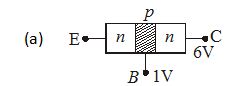
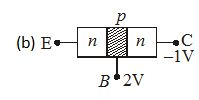
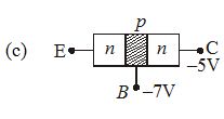
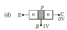
Ans (a)
2.
The distance between two atoms in contact is known as
(a) lattice parameter
(b) atomic radius
(c) number of constituent
(d) packing factor.
Ans (a)
3.
The value of a
(a) is always infinity
(b) is always less than 1
(c) lies between 50 and 150
(d) is always greater that 150.
Ans (b)
4.
The relation between a and b is given by
(a) \beta =\frac{\alpha }{{1-\alpha }}
(b) \displaystyle \alpha -\beta
(c) \beta =\frac{\alpha }{{1+\alpha }}
(d) \alpha =\frac{1}{\beta }.
Ans (a)
5.
The value of current gain in CB amplifier is
(a) greater than one
(b) less or greater than one
(c) less than one
(d) none of the above.
Ans (c)
6.
For a transistor IC = 25 mA and Ib = 1 mA. What is the value of a?
(a) 25/25
(b) 26/25
(c) 24/25
(d) 25/26.
Ans (d)
7.
What is the process of superimposing signal frequency on the carrier frequency called?
(a) detection
(b) reception
(c) modulation
(d) transmission.
Ans (c)
8.
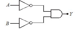
To get an output Y = 1 from circuit in figure the input must be
A B C
(a) 0 1 0
(b) 1 0 0
(c) 1 0 1
(d) 1 1 0
Ans (c)
9.
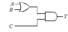
What is the output Y of the gate circuit shown in the figure
(a) \bar{A}.\bar{B}
(b) \overline{\overline{{A.B}}}
(c) \overline{{A.B}}
(d) none of these.
Ans (a)
Practice Questions (JEE Main Level)
Comprehension Based Question (1 to 3)
A transistor has a base current of 0.08 mA and the emitter current is 10 mA. Determine
1.
the collector current
(a) 6.92 mA
(b) 0.35 mA
(c) 43.6 mA
(d) 9.92 mA
Ans (d)
2.
current gain in CB configuration and
(a) 1.453
(b) 0.234
(c) 0.992
(d) 2.349
Ans (c)
3.
current gain b in CE configuration?
(a) 124
(b) 321
(c) 854
(d) 547
Ans (a)
4.
The collector current for a transistor is 6.6 mA, and its current gain a is 0.95. Determine IBand b.
(a) 0.35 mA, 0.3
(b) 0.35 mA, 25
(c) 0.35 mA, 34
(d) 0.35 mA, 19
Ans (d)
Comprehension Based Question (5 and 6)
For a CB amplifier, the input resistance is 800 and the output resistance is 600 kW.
5.
Determine the voltage gian if the emitter current is 12 mA and a = 0.97.
(a) 735
(b) 727
(c) 758
(d) 795
Ans (b)
6.
What is the power gain?
(a) 770
(b) 754
(c) 700
(d) 706
Ans (d)
7.
The power gain for CB amplifier is 800, and the voltage amplification factor is 840. Find the collector current when the base current is 1.2 mA.
(a) 70 mA
(b) 13 mA
(c) 24 mA
(d) 20 mA
Ans (c)
8.
The current gain of a transistor is 0.95. What would be the change in collector current corresponding to a change of 0.4 mA in the base current in CE configuration?
(a) 7.59 mA
(b) 7.28 mA
(c) 7.6 mA
(d) 7.005 mA
Ans (c)
9.
The current gain of transistor in CB configuration is 0.98. Find the change in collector current corresponding to a change of 5.0 mA in the emitter current. What would be the change in base current?
(a) 4.9 mA, 0.1 mA
(b) 4.9 mA, 0.5 mA
(c) 4.9 mA, 0.67 mA
(d) 4.9 mA, 2.54 mA
Ans (a)
Practice Questions (JEE Advance Level)
Lorem ipsum dolor sit amet, consectetur adipiscing elit. Ut elit tellus, luctus nec ullamcorper mattis, pulvinar dapibus leo.