Video Lecture

Theory For Making Notes

Lorem ipsum dolor sit amet, consectetur adipiscing elit. Ut elit tellus, luctus nec ullamcorper mattis, pulvinar dapibus leo.

Practice Questions (Level-1)

1.

A semiconductor has the electron concentration 0.45 × 10¹² m–3 and hole concentration 5 × 10²⁰ m–3. Find its conductivity. Given: electron mobility = 0.135 m2V–1s–1 and hole mobility = 0.048 m2v–1s–1; e = 1.6 × 10⁻¹⁹ coulomb.

(a) 1.548 \displaystyle \Omega m–1

(b) 1.224 \displaystyle \Omega m–1

(c) 3.845 \displaystyle \Omega m–1

(d) 0.456 \displaystyle \Omega m–1

Ans (c)

2.

When the voltage drop across a pn junction diode is increased from 0.70V to 0.71 V, the change in the diode current is 10 mA. What is the dynamic resistance of the hole?

(a) 27 \displaystyle \Omega

(b) 20 \displaystyle \Omega

(c) 4 \displaystyle \Omega

(d) 1 \displaystyle \Omega

Ans (d)

3.

In a p type semiconductor the acceptor level is situated 57 meV above the valence band. The maximum wavelength of light required to produce a hole will be

(a) 57 × 10–3Å                                

(b) 11.61 × 10⁻³³ watt                 

(c) 57 Å    

(d) 217100 Å.

Ans  (d)

4.

The band of maximum energy in which electrons are present is called

(a) valence band                         

(b) forbidden band                    

(c) conduction band                   

(d) fermi band.

Ans  (a)

5.

The relation between the number of free electrons in semiconductors (n) and its temperature (T) is

(a) n \displaystyle \propto T                           

(b) n\propto \sqrt{T}                                        

(c) n \displaystyle \propto T3/2                       

(d) n \displaystyle \propto T2.

Ans  (c)

6.

The electron mobility in an n type germanium is 3900 cm2/V-s and its conductivity is 6.24 mho cm–1, then the impurity concentration will be

(a) 1016/cm3                         

(b) 1015/cm3                                  

(c) 1013/cm                           

(d) 1012/cm3.

Ans (a)

7.

Polymers are the substance which are

(a) amorphous in nature                  

(b) semi-solids

(c) crystalline in nature                                                

(d) none of these.

Ans (d)

8.

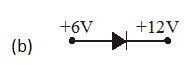
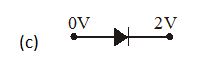
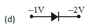
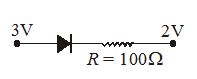
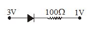
In which case is the junction diode forward biased

Ans (d)

9.

Acceptor type or p type semiconductor is formed by adding impurity of valency

(a) 6  

(b) 5  

(c) 4  

(d) 3.

Ans(d)

10.

The ripple factor in a full-wave rectifier is

(1) 0.48    

(2) 1.21    

(3) 0.62    

(4) 1.0.

Ans (a)

11.

Assuming that the junction diode is ideal, the current in arrangement as shown in figure is

(a) 2 mA  

(b) 10 mA                                       

(c) 20 mA

(d) 30 mA.

Ans (b)

Practice Questions (Level-2)

1.

The number density of electrons and holes in intrinsic silicon at a given temperature is 4.94 × 1010 cm–3. Calculate the resistivity and conductivity of the silicon. Given electron mobility = 100 cm2V–1s–1 and hole mobility –1000 cm2 V–1 s–1.

(a) 9 × 10⁴ \displaystyle \Omega cm, 0.5 × 10⁻⁶ s cm–1

(b) 9 × 10⁴ \displaystyle \Omega cm, 11.1 × 10⁻⁶ s cm–1

(c) 2 × 10⁴ \displaystyle \Omega cm, 10.4 × 10⁻⁶ s cm–1

(d) 9 × 10⁴ \displaystyle \Omega cm, 7.15 × 10⁻⁶ s cm–1

Ans  (b)

2.

Determine the number density of donor atoms which have to be added to an intrinsic germanium to produce an n-type semiconductor of conductivity 0.06 sm–1. Given the mobility of electrons = 0.39 m2v–1s–1. Neglect the contribution of the diode?

(a) 87 × 1016 m–3

(b) 34 × 1016 m–3

(c) 0.45 × 10¹⁶ m–3

(d) 96 × 1016 m–3

Ans (d)

3.

A pn junction is designed to withstand currents upto a maximum current of 10 mA. A resistance of 200W is connected in series with it. When forward biased, the diode has a potential drop of 0.5V which is assumed to be independent of current. Find the maximum voltage of the battery to forward bias the diode.

(a) 1.4V

(b) 9.2V

(c) 2.5V

(d) 3.4V

Ans (c)

4.

The safe limits of temperature for germanium and silicon care

(a) 8 × 10² °C and 2 × 10² °C

(b) 80°C and 2 × 10² °C

(c) 2 × 10³ °C and 80°C                                                  

(d) 2 × 10² °C and 800°C.

Ans (b)

5.

The potential barrier of silicon at 30° C is 0.7 eV, then its value at 13° C will be

(a) 0.9 eV

(b) 0.6 eV                                       

(c) 0.67 eV                                      

(d) 0.7 eV.

Ans (c)

6.

A solid which is not transparent to visible light and shoes electrical conductivity decreases with temperature is formed by

(a) ionic bonding                                               

(b) van der wall bonding                            

(c) metallic  bonding                  

(d) covalent bonding.

Ans (c)

7.

In the arrangement shows in figure below, the current through diode is

(a) 1 mA  

(b) 10 mA                                       

(c) 20 mA

(d) zero.

Ans (c)

8.

On doping germanium with donor atoms of density 1017 cm–3, its conductivity in mho cm–1 will be —— if m = 3800 cm2/V-s and ni = 2.5 × 1013 cm–3

(a) 240

(b) 180     

(c) 120      

(d) 60.8

Ans  (c)

9.

The number of densities of electrons and holes in pure silicon at 27°C are equal and its value is 1.5 × 10¹⁶ m–3. On doping with indium, the hole density increases to 4.5 × 10²² m–3. The electron density in doped silicon will be

(a) 108 m–3                                      

(b) 107 m–3                                                         

(c) 50 × 109 m–3                             

(d) 5 × 10⁹ m–3.

Ans  (c)

10.

A silicon specimen is made into a p type semiconductor by doping, on an average one indium atom per 5 × 10⁷ silicon atom. If the number density of atom in the silicon specimen is 5 × 1028 atom/m3 then the number of acceptor atoms in silicon per cm3 will be

(a) 1.0 × 10¹⁵                                  

(b) 2.5 × 1036                                                   

(c) 2.5 × 1030                                  

(d) 1.0 × 10³.

Ans  (d)

11.

Two identical p-n junction may be connected in series with a battery in three ways as shown in figure. The potential drop across the pn junction are equal in

(a) circuit 3 and circuit 1                    

(b) circuit 1 and circuit 2

(c) circuit 2 and circuit 3                    

(d) only circuit 1.

Ans  (c)

12.

For the given circuit shown is figure, to act as full-wave rectifier, the ac input should be connected across … and then dc output would appear across …

(a) A B, C D                        

(b) A C, B D                        

(c) B C, A D                       

(d) B D, A C.

Ans (d)