Video Lecture
Theory For Making Notes
Energy Band Theory
In the case of an isolated atom all the electrons are restricted to have a certain amount of energy only which are called their energy levels. But in the case of a solid where a large number of atoms are closely packed, an atom is surrounded by a large number of other atoms due to their closeness they interact with each other as a result of which the energy of the outermost electrons is modified. This modification is significant for the electrons in the outermost shell because these electrons experience large influence by the electric field of neighboring atoms. Therefore in the case of a solid the energy of the electrons of a certain shell is not unique but it lies in a range called the energy band of that shell. Hence an energy band is a group of energy levels. Every band contains a large number of energy levels ( \displaystyle \sim{{10}^{{23}}}) which are closely packed and each energy level can contain only two electrons.
Let’s take an example
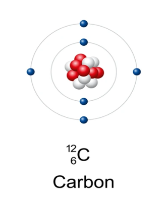
Consider the carbon atom which has 6 atomic number. Hence its configuration is \displaystyle 1{{s}^{2}}2{{s}^{2}}2{{p}^{2}}. Its energy level diagram contains single energy level corresponding to \displaystyle 1{{s}^{2}},2{{s}^{2}},\And \text{ }2{{p}^{2}} as shown below

When a solid of carbon is considered it is found that corresponding to 2s and 2p there are energy bands present as shown in the diagram.
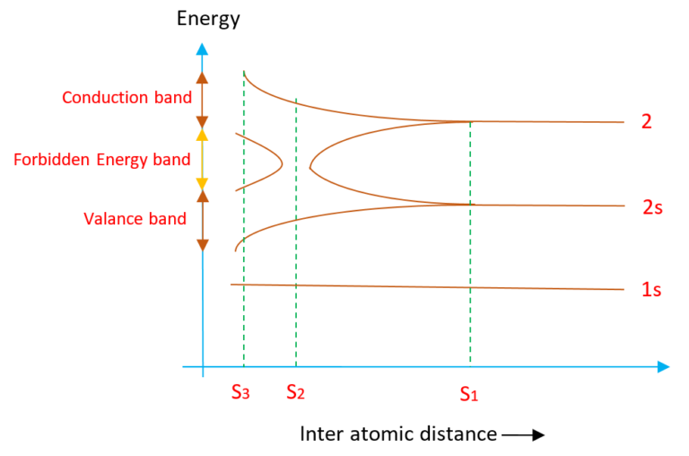
This formation of energy bands shows the change in energy of the outermost electrons. The width of the energy bands increases with decrease in the inter atomic distance which shows that as the inter atomic distance decreases the energy of the outermost electrons will change more and more. According to the diagram, upto inter atomic distance \displaystyle {{S}_{1}}there is no interaction between the atoms hence they behave like isolated atoms and there is no change in the energy levels. But as the inter atomic distance decreases further the energy levels of 2s and 2p get splited to form energy band. As the inter atomic distance reaches a distance \displaystyle {{S}_{2}}the width of the energy bands of 2s and 2p becomes so large that they start overlapping. At this stage the energy of their electrons start overlapping and hence now we can not distinguish between the electrons of the 2s and 2p orbits. We know that in L shell a total of 8 electrons can be accommodated but there are 4 electrons present in case of carbon atom. Hence there are unfilled energy levels present there . So we find that with further decrease in the inter atomic distance upto \displaystyle {{S}_{3}}a further splitting occur between the filled and unfilled energy levels of the outermost `L’ shell.
All the unfilled energy levels acquire a little higher energy state and form a band called conduction band. All filled energy levels start forming a band called valance band and the distance between the valance band and conduction band is called forbidden energy band or energy gap. Hence in a solid the energy is divided into three categories:
Conduction band
The band which contain the energy levels of the free electrons in a solid. That is the energy of all free electrons lie in this band. It is also defined as the lowest unoccupied band in the energy band diagram. The electrons lying in this band are used to conduct electrical current.
Valance band
All valance electrons have their energy lying in the range called valance band. This is also defined as the highest occupied band in the energy band diagram. While remaining in this band the electron is always immobile.
Forbidden band
The distance between the top of the valance band and the bottom of the conduction band is called forbidden energy band. No electron can exist in this band. The width of this band is a measure of the energy required to make a valance electron free.
Difference between Insulators, semiconductors & good conductors on the basis of energy band theory
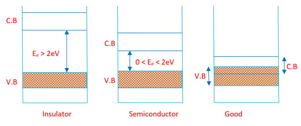
Insulator
In the case of an insulator the energy gap between the conduction band and valance band is very large usually more than 2ev. Due to this large energy gap the valance electrons cannot jump easily from valance band to the conduction band. In order to make a insulator conducting a large amount of energy is required to be supplied to the valance electrons. This energy can be supplied bu either increasing temperature or by applying a high potential difference across the insulator.
Example: Glass with Eg = 10ev.
Semiconductor
In the case of a semiconductor the energy gap is very small as a result the valance electrons can easily gain sufficient energy to jump into the conduction band. some time even at room temperature they are able to jump into the conduction band and become free. But at very low temperatures the semiconductor behaves like an insulator.
Example: Silicon with Eg = 1.1ev , Germanium with Eg = 0.7ev.
Conductors
In good conductors there is no energy gap and there is a overlapping of the valance band and the conduction band. Due to this the electrons are so free that they can go into the conduction band without requiring any energy. Hence for a good conductor no energy is required to make it conduction whereas in insulators and semiconductors energy is required to make them conducting.
Example: Copper,aluminum,iron etc.
Types Of Semiconductors on the bases of Doping
Doping is the addition of impurity in the semiconductor. So on this bases there
Intrinsic Semiconductor
Those semiconductors which have no impurity i.e. they are pure semiconductors. For example silicon and germanium. These are tetravalent and have four electrons in their valance orbit. These four electrons make covalent bonding with four electrons of the neighboring atoms. In this way there is no free electron in their conduction band as shown in the figure given below.
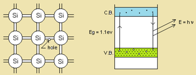
When energy is supplied to the valance electrons they get excited and start jumping from valance band to the conduction band. When an electron jumps into the conduction band it leave behind a vacancy called a hole. Therefore the number of holes will always be equal to the number of free electrons in this semiconductor. The atom with the hole has now only seven electrons and hence it try to complete its octave for which it capture one electron from any of the neighboring atom. This process creates one hole in the neighboring atom, due to which this atom also try to capture one electron and hence this process will go on and the hole keeps on shifting from one atom to other atom. On applying a potential difference the hole is found to move towards negative terminal and hence we can assume that the hole are having positive charge. This means that in a semiconductor there are two types of currents one which is produced by the motion of the free electron and second is the current due to the motion of the hole. Hence if I is the total current Ip is the current due to hole and In is the current due to the free electrons then \displaystyle I={{I}_{p}}+{{I}_{n}}. & \displaystyle {{N}_{n}}={{N}_{p}}.
If any free electron recombined with a hole then the excess energy of the electron comes out as radiation. In the case of silicon and germanium these radiation are in the infrared region. The same radiation is in the visible region in gallium arsenide, which is used in making L.E.D.
Extrinsic Semiconductor
The conductivity of a pure semiconductor is small and hence they can not be used directly. Therefore to make them useful, their conductivity is increased by adding impurity in them by the method called doping. The new semiconductor is called doped or extrinsic semiconductor. The amount of impurity used is called doping level which is of the order of \displaystyle 1:{{10}^{6}} i.e. in \displaystyle {{10}^{6}} atoms of intrinsic semiconductor one impurity atom should be added. Depending on the type of impurity used there are two types of extrinsic semiconductors
- n-type semiconductor
- p-type semiconductor
n-type extrinsic semiconductor
If in the intrinsic semiconductor the impurity used is pantavalent then the new semiconductor formed is called c type of semiconductor. Let the impurity used is arsenic then four of its 5 valance electrons will fall in the bonding with the electrons of the silicon whereas the fifth electron remain without any bonding. The energy level of this fifth electron lies just below the bottom of conduction band. The difference between the energy level of this electron and the bottom of the conduction band is of the order of 0.01ev. This electron gains this small amount of energy even from room temperature and hence it becomes free. In this way with each arsenic
atom we add one free electron in the semiconductor due to which the conductivity of the semiconductor will increase. As this impurity atom is donating its one electron for the purpose of conduction therefore it is called donor impurity. The energy level of the fifth electron is called the donor level. As the negatively charged electrons are the majority current carriers in this semiconductor therefore it is called n-type semiconductor
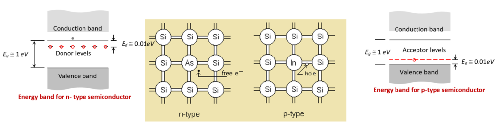
p-type semiconductor
If in the intrinsic semiconductor the impurity used is trivalent then the new semiconductor formed is called p-type semiconductor. Let the impurity used is indium then all three valance electrons of it will fall in the covalent bonding with the electrons of the silicon atom where as the fourth electron of the silicon atom will remain with a vacancy i.e. a hole. Due to which the silicon atom with this hole will try to capture an electron from the neighboring atom. Bu doing this it fills its own hole but creates a new hole in the neighboring atom in this way the hole will start moving from one atom to other as if it is free. As we know that the hole moves in a direction opposite to the electrons and hence it acts like a free positive charge therefore now the conductivity of the semiconductor will increase by the addition of the holes. As by adding this impurity now a tendency of accepting the electron by the silicon atom is increased therefore this type of impurity is called acceptor impurity. In this semiconductor as the +ve charged holes are the majority current carriers therefore this type of semiconductor is called p-type semiconductor.
Electrical conductivity of a semiconductor
We know that inside a semiconductor the current flows due to the motion of the free electrons and also due to the motion of the holes .
Hence total current I is given by
\displaystyle I={{I}_{p}}+{{I}_{n}} —(1)
where \displaystyle {{I}_{n}} is the current due to negative charges i.e. electrons and \displaystyle {{I}_{p}} is current of positive charges i.e. holes.
Also we know that \displaystyle {{I}_{p}}=\text{ }{{n}_{p}}eA{{V}_{{dp}}} & \displaystyle {{I}_{n}}=\text{ }{{n}_{n}}eA{{V}_{{dn}}}
where \displaystyle {{n}_{n}} and \displaystyle {{n}_{p}} represents the free electron’s density and holes density respectively. And \displaystyle {{V}_{{dp}}} & \displaystyle {{V}_{{dn}}} represents the drift velocity of the holes and the electrons.
Assuming ohm’s law is valid hence net current \displaystyle I=\frac{V}{R}
put \displaystyle R=\frac{{\rho l}}{A} { }and{ }V=El in the above equation
we get \displaystyle I=\frac{{El}}{{\left( {\frac{{\rho l}}{A}} \right)}} ( here E is the net electric field inside the conductor )
\displaystyle \Rightarrow \text{ }I=\frac{{EA}}{\rho }
hence using equation (1) we can write \displaystyle \text{ }I=\frac{{EA}}{\rho }={{I}_{n}}+{{I}_{p}}
\displaystyle \Rightarrow \text{ }\frac{{EA}}{\rho }={{n}_{n}}eA{{v}_{{dn}}}+{{n}_{p}}eA{{v}_{{dp}}} (cancel A and cross multiply E)
\displaystyle \Rightarrow \text{ }\frac{1}{\rho }={{n}_{n}}e\frac{{{{v}_{{dn}}}}}{E}+{{n}_{p}}e\frac{{{{v}_{{dp}}}}}{E}
here put \displaystyle 1/\rho =\sigma ( conductivity of semiconductor) and also \displaystyle {\frac{{{{v}_{{dn}}}}}{E}={{\mu }_{n}}\text{ and }\frac{{{{v}_{{dp}}}}}{E}={{\mu }_{p}}} in the above equation
so we get
\displaystyle \sigma ={{n}_{n}}e{{\mu }_{e}}+{{n}_{p}}e{{\mu }_{p}}
where \displaystyle {{\mu }_{n}} & \displaystyle {{\mu }_{p}} are called the mobility of free electrons and holes. And it is defined as the drift velocity per unit electric field applied.
For an intrinsic semiconductor \displaystyle {{n}_{p}}={{n}_{n}}=n (say)
hence \displaystyle \sigma =en\text{ }[{{\mu }_{n}}+{{\mu }_{p}}]
For a p type semiconductor \displaystyle {{n}_{p}}\gg {{n}_{n}}
hence \displaystyle \sigma =e{{n}_{p}}{{\mu }_{p}}
For a n type semiconductor \displaystyle {{n}_{n}}\gg {{n}_{p}} hence \displaystyle \sigma =e{{n}_{n}}{{\mu }_{n}}
Law Of Mass Action
The law of mass action states that the product of number of electrons in the conduction band and the number of holes in the valence band is constant at a fixed temperature and is independent of amount of donor and acceptor impurity added.
Let ne = number of electrons in the conduction band
and np = number of holes in the valance band
According to the law of mass action \displaystyle {{n}_{e}}\times {{n}_{p}}={{n}_{i}}^{2}.
where \displaystyle {{n}_{i}}= intrinsic carrier concentration
For Intrinsic semiconductor \displaystyle {{n}_{p}}={{n}_{n}}=n (say)
hence the equation of law becomes \displaystyle {{n}^{2}}=\text{ }{{n}_{i}}^{2}
The law of mass action is applied for both intrinsic and extrinsic semiconductors.
For extrinsic semiconductor the law of mass action states that the product of majority carriers and minority carriers is constant at fixed temperature and is independent of amount of donor and acceptor impurity added.
Let’s say in n type semiconductor electrons are in majority and holes are in minority
so while applying the law of mass action i.e. \displaystyle {{n}_{e}}\times {{n}_{p}}={{n}_{i}}^{2}.
\displaystyle {{n}_{e}} represents the number of free electrons in the conduction band
& \displaystyle {{n}_{p}} represents the number of holes in the valance band.
So the equation tells that if the number of free electrons in the conduction band increases the number of holes in the valance band decreases. Therefor the product of number of free electrons and holes remains constant at a fix temperature.
A similar explanation can be done for p-type of semiconductor.
Illustration
Pure Si at 300 K has equal concentration of free electrons ( \displaystyle {{n}_{e}}) and holes ( \displaystyle {{n}_{h}}) as \displaystyle 2.8\text{ }\times \text{ }{{10}^{{16}}}{{m}^{{3}}}. Doping by trivalent impurity increases hole concentration to \displaystyle 5.0\text{ }\times \text{ }{{10}^{{22}}}{{m}^{{3}}}. Calculate \displaystyle {{n}_{e}} in doped silicon.
Solution
Here {{n}_{i}}=2.5\times {{10}^{{16}}}{{\text{m}}^{{-3}}},\,{{n}_{h}}=5.0\times {{10}^{{22}}}{{\mathbf{m}}^{{-3}}}.
Using, {{n}_{e}}=\frac{{n_{i}^{2}}}{{{{n}_{h}}}}=\frac{{(2.8\times {{{10}}^{{16}}})}}{{5.0\times {{{10}}^{{22}}}}} =1.57\times {{10}^{{10}}}{{\text{m}}^{{-3}}}.
Illustration
The number densities of electron and holes in pure silicon at {{27}^{o}}C are equal and its value is \displaystyle 1.5\text{ }\times \text{ }{{10}^{{16}}}{{m}^{{3}}}. On doping with indium, the hole density increases to \displaystyle 4.5\text{ }\times \text{ }{{10}^{{22}}}{{m}^{{3}}}. What is the type of semiconductor ? What is the electron density in doped silicon ?
Solution
Since in a doped semiconductor \displaystyle {{n}_{p}}\gg {{n}_{n}}, So the semiconductor is of p-type semiconductor. The electron density in doped semiconductor,
ne = \frac{{n_{i}^{2}}}{{{{n}_{h}}}} = \frac{{{{{(1.5\times {{{10}}^{{16}}})}}^{2}}}}{{4.5\times {{{10}}^{{22}}}}} = \displaystyle 5\text{ }\times \text{ }{{10}^{{9}}}{{m}^{{3}}} .
Illustration
A Ge specimen is doped with Al. The concentration of acceptor atoms is \displaystyle \approx {{10}^{{21}}} atoms/{{m}^{3}}. Given that the intrinsic concentration of electrons in the specimen is \displaystyle \approx {{10}^{{19}}} /{{m}^{3}}. . The new electron concentration is
(A) \displaystyle \approx {{10}^{{17}}} /{{m}^{3}}.
(B) \displaystyle \approx {{10}^{{15}}} /{{m}^{3}}.
(C) \displaystyle \approx {{10}^{{4}}} /{{m}^{3}}.
(D) \displaystyle \approx {{10}^{{20}}} /{{m}^{3}}.
Solution
When Ge specimen is doped with Al, then concentration of acceptor atoms is also called concentration of holes.
Using formula
n_{i}^{2}={{n}_{e}}{{n}_{h}}
concentration of electron hole pair = \displaystyle {{n}_{i}}={{10}^{19}} / {{m}^{3}}
\displaystyle {{n}_{e}} = concentration of electrons
\displaystyle {{n}_{h}}= concentration of holes = \displaystyle \approx {{10}^{{21}}} atoms/{{m}^{3}}
or \displaystyle {{\left( {{{{10}}^{{19}}}} \right)}^{2}}=\text{ }{{10}^{{21}}}\times {{n}_{e}}
\displaystyle {{n}_{e}}=\text{ }{{10}^{{17}}}/{{m}^{3}}
hence option (A) is correct
Illustration
For a semiconductor with electron concentration \displaystyle 7\text{ }\times \text{ }{{10}^{{18}}}{{m}^{{-3}}} and hole concentration \displaystyle 9\text{ }\times \text{ }{{10}^{{19}}}{{m}^{{-3}}}, calculate the conductivity. Given: electron mobility = \displaystyle 3.2\text{ }{{m}^{2}}{{V}^{{1}}}{{s}^{{1}}} and hole mobility = \displaystyle 0.02\text{ }{{m}^{2}}{{V}^{{1}}}{{s}^{{1}}}.
Solution
Here {{n}_{e}}=7\times {{10}^{{18}}}{{\text{m}}^{3}},{{n}_{h}}=9\times {{10}^{{19}}}{{\text{m}}^{{-3}}}
{{\text{ }\!\!\mu\!\!\text{ }}_{\text{e}}}=\text{3}\text{.2}{{\text{m}}^{\text{2}}}{{\text{V}}^{{-\text{1}}}}{{\text{s}}^{{-\text{1}}}}\text{,}\,{{\text{ }\!\!\mu\!\!\text{ }}_{\text{h}}}=\text{0}\text{.02}{{\text{m}}^{\text{2}}}{{\text{V}}^{{-\text{1}}}}{{\text{s}}^{{-\text{1}}}}
Now, conductivity \sigma =e[{{n}_{e}}{{\mu }_{e}}+{{n}_{h}}{{\mu }_{h}}]
=1.6\times {{10}^{{19}}}[7\times {{10}^{{18}}}\times 3.2+9\times {{10}^{{19}}}\times 0.02]
=\text{3}\text{.872S}{{\text{m}}^{{-\text{1}}}}\text{.}
Illustration
Current density, J in extrinsic or impurity added semi conductor is given as
(1) J = \displaystyle {{n}_{e}}e ( {{v}_{e}}-{{v}_{h}})
(2) J = e ( {{n}_{e}}{{v}_{e}}+{{n}_{h}}{{v}_{h}})
(3) J = \displaystyle {{n}_{e}}{{n}_{e}}
(4) J = {{n}_{e}}{{n}_{h}} \frac{{{{v}_{e}}}}{{{{v}_{h}}}}
Solution
\displaystyle J=\frac{{{{I}_{e}}+{{I}_{h}}}}{A}=\frac{{eA{{n}_{e}}{{v}_{e}}+eA{{n}_{h}}{{v}_{h}}}}{A}=e\text{ }({{n}_{e}}{{v}_{e}}+{{n}_{h}}{{v}_{h}}).
Hence option (2) is correct
Illustration
A semiconductor is known to have an electron concentration of \displaystyle \text{8}\times {{10}^{{13}}}c{{m}^{{-3}}} and a hole concentration of \displaystyle \text{5}\times {{10}^{{12}}}c{{m}^{{-3}}}. (a) Is the semiconductor n-type or p-type. (b) What is the resistivity of the sample if the electron mobility is 23000 \displaystyle c{{m}^{2}}/Vs and hole mobility is 100 \displaystyle c{{m}^{2}}/Vs?
Solution
Here {{n}_{e}}=8\times {{10}^{{13}}}\text{c}{{\text{m}}^{{-3}}},\ {{n}_{h}}=5\times {{10}^{{12}}}\text{c}{{\text{m}}^{{-3}}},
{{\mu }_{e}}=23000\text{c}{{\text{m}}^{2}}{{\text{V}}^{{-1}}}{{\text{s}}^{{-1}}},\ {{\mu }_{h}}=100\text{c}{{\text{m}}^{2}}{{\text{V}}^{{-1}}}{{\text{s}}^{{-1}}}
(a) As \displaystyle {{n}_{e}}\text{}>{{n}_{h}}, the semiconductor must be n-type.
(b) Resistivity, \rho =\frac{1}{{e({{n}_{e}}{{\mu }_{e}}+{{n}_{h}}{{\mu }_{h}})}}
hence \rho =\frac{1}{{1.6\times {{{10}}^{{-19}}}(8\times {{{10}}^{{13}}}\times 23\times {{{10}}^{3}}+5\times {{{10}}^{{12}}}\times {{{10}}^{2}})}}\Omega \text{cm}
\rho = 3.395\ \Omega \text{cm}.
Illustration
Determine the number density of donor atoms which have to be added to an intrinsic germanium semiconductor to produce an n-type semiconductor of conductivity \displaystyle 5{{\Omega }^{{-1}}}c{{m}^{{-1}}}, given that the mobility of electron in n-type Ge is 3900 \displaystyle c{{m}^{2}}/Vs. Neglect the contribution of holes to conductivity.
Solution
Here \sigma =5{{\Omega }^{{-1}}}\text{c}{{\text{m}}^{{-1}}},{{\mu }_{e}}=3900\text{c}{{\text{m}}^{2}}{{\text{v}}^{{-1}}}{{\text{s}}^{{-1}}},{{n}_{e}}=?
As we can neglect the contribution of holes to conductivity,
therefore \sigma =\frac{1}{\rho }=e{{n}_{e}}{{\mu }_{e}}
Hence the number density of donor atoms is {{n}_{e}}=\frac{\sigma }{{e{{\mu }_{e}}}}
or {{n}_{e}}=\frac{5}{{1.6\times {{{10}}^{{-19}}}\times 3900}}
therefore {{n}_{e}} =8.01\times {{10}^{{15}}}\text{/c}{{\text{m}}^{3}}.
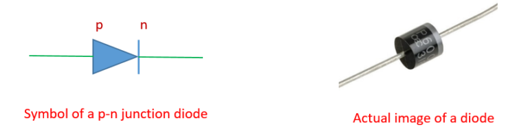
p-n Junction Diode
When a p and n type of semiconductor are joined together they form p-n junction diode. For making a p-n junction diode the p and n type of semiconductors are fused together after melting. The imaginary line between the p and n type of semiconductor is called p-n junction. When a p-n junction is made then diffusion of charges starts from the region of high concentration to the region of low concentration. Hence the diffusion of holes will start from p region to n region whereas the electrons will move in the opposite direction this movement of charges produces a net current across the p-n junction from p to n region.
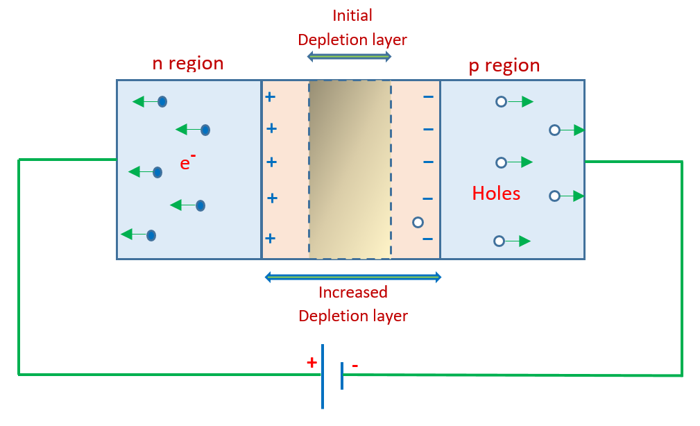
As any hole diffuse into the n region it leave behind a negative charge in the p region whereas when an electron diffuse into the p region it leave behind a positive charge in the n region. Due to this action a potential difference is produced across p-n junction as shown in the diagram (a) which shows the diffusion of charges.
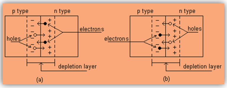
This potential difference opposes the diffusion of charges across the p-n junction and hence it is called potential barrier.
Apart from producing a potential barrier, the diffusion of holes and electrons in opposite direction results in a large number of recombination of holes and electrons near the p-n junction. Therefore near the p-n junction a region is formed in which the free charge density becomes negligible, this region is called depletion layer.
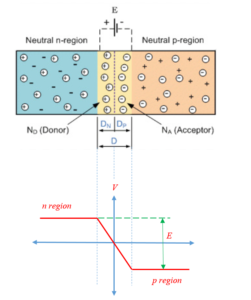
Along with diffusion there is another process called drift that also proceeds across the p-n junction in a direction opposite to that of the diffusion. Consider the part of the depletion layer in the p region where with free hole there are also a few free electrons be present. Whereas in the part of the depletion layer in the n region apart from the free electrons there are also a few free holes be present. These electrons and holes under the influence of the electric field of the depletion layer move towards the n region and p region respectively as shown in the diagram (b) given above. This movement of electrons and holes is taking place opposite to that of the diffusion and this is what we called as drift. The drift consists of the movement of minority carriers of both the regions across p-n junction and produces a net current from n to p region . The width of the depletion layer is of the order of 1mm. Whereas due to the potential barrier the electric field produced in the depletion layer is of the order of a few tenth of 1volt like 0.5volt. Hence the electric field in the depletion layer can be found as follows:
\displaystyle E=\frac{V}{d}
\displaystyle E=\frac{{0.5}}{{{{{10}}^{{-6}}}}} Volt/m.
\displaystyle E=5\times {{10}^{5}}volt/m.
Under these conditions the drift current and the diffusion current balance with each other and there is no net current passing across the p-n junction.
BIASING OF P-N JUNCTION DIODE
When a battery is applied across the p-n junction diode it is said to be biased. There are two types of biasing
- Forward biasing
- Reverse biasing
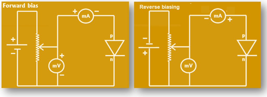
Forward biasing

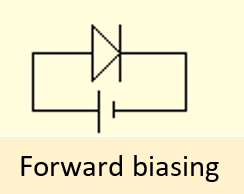
When the p region of the diode is connected with the higher potential i.e. the positive terminal and the n region is connected to the lower potential i.e. negative terminal the diode is said to be forward biased. When battery is applied in this way then the positive terminal of the battery repel the holes of the p region and the negative terminal of the battery repel the electrons of the n region. As a result of which the hole and electrons are forced to move towards the p-n junction , due to which the width of the depletion layer decreases. Also in this case the potential difference applied has a direction opposite to that of the potential barrier. Due to which the magnitude of the potential barrier decreases and hence the diffusion can be started if the applied potential difference is more that the potential barrier. Hence the current flow is principally due to majority charge carriers and is large (mA).
Reverse biasing
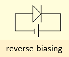
When the p region of the diode is connected with the lower potential i.e. negative terminal and the n region is connected to the higher potential i.e. the positive terminal ,diode is said to be reverse biased. When battery is applied in this way then the positive terminal of the battery attract the electrons of the n region and the negative terminal of the battery attract the holes of the p region. As a result of which the electrons and hole are forced to move away from the p-n junction , due to which the width of the depletion layer increases. Also in this case the potential difference applied has a direction same as that of the potential barrier. Due to which the magnitude of the potential barrier increases and hence the diffusion can not take place at any applied potential difference. So, the reverse bias current will be due to the minority carriers (\sim\mu \mathbf{A}) and it is very small as compared to the majority carriers, the reverse bias current is small.
Characteristic of a p-n junction diode
Dynamic Resistance
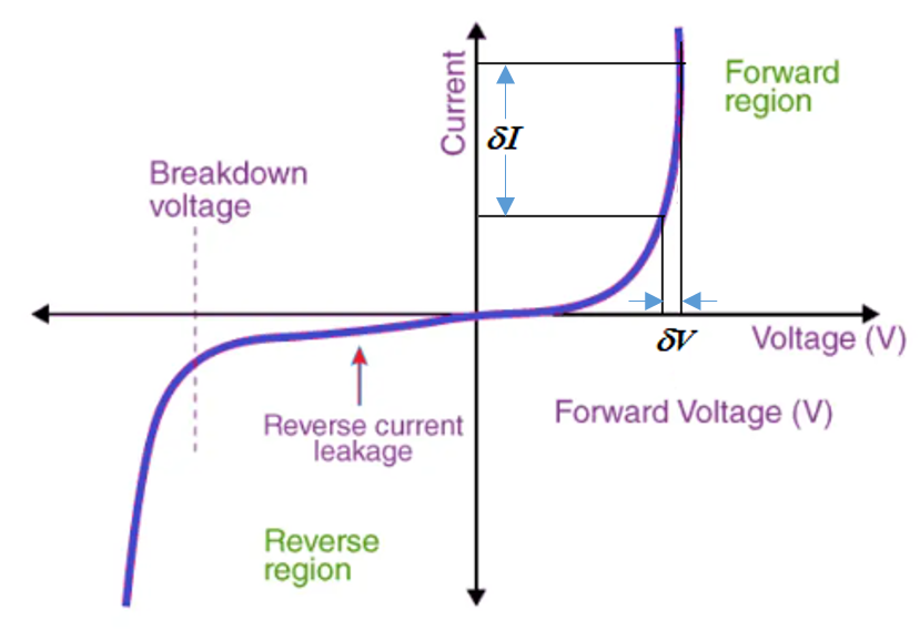
\displaystyle {{r}_{d}}=\frac{{\delta V}}{{\delta I}}
It is the graph drawn between the voltage applied and the current passing through the diode. It shows that when forward biasing voltage is applied across the diode,there is initial slow increase in the forward current till the biasing voltage is less than the potential barrier. It is because of the fact that a little energy is supplied by the applied potential where as some of the free electrons acquire energy due to surrounding temperature also as a result their total energy becomes sufficient to over come a large potential barrier. And as soon as the applied potential exceeds the potential barrier a sudden rise of current is shown in the graph which indicates that after over coming the potential barrier the diode becomes a very good conductor of negligibly small resistance. This resistance of the diode is called dynamic resistance as its value depends on the part of the forward characteristic chosen , theoretically the resistance of a diode in the forward biasing is taken as zero.
When the reverse biasing is applied it is found that there is a very small reverse current across the p-n junction which is taken as zero theoretically. This situation remains there till the reverse potential reaches a certain value called breakdown potential, beyond which when the voltage is increased there is a sharp rise in the reverse current and the graph becomes almost parallel to the current axis. This phenomena is called breakdown of the
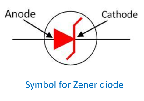
diode, and the diodes used in the breakdown region of the reverse characteristic are called zener diodes. This breakdown characteristic shows that even when the current through the zener diode changes the voltage across it remains almost constant. Due to this these diodes are also called reference diodes. The resistance of a zener diode is negligibly small.
BREAKDOWN OF DIODES
Breakdown of the diodes is of two types
- Avalanche breakdown
- Zener breakdown.
Avalanche breakdown
When a sufficiently high reverse biasing voltage is applied across the diode some of the electrons in the depletion region becomes free and gain kinetic energy due the electric field produced by the potential barrier in the depletion region. As these electrons hits other electrons due to collisions new free electrons are formed then all these electrons start accelerating and gain kinetic energy and by collisions produce more free electrons. In this way the number of free electrons gets multiplied and suddenly we get a large number of pair of free electrons and holes which increases the conductivity of the diode suddenly and hence the current increases sharply. This type of breakdown occur mostly in highly doped diodes.
Zener breakdown
When a reverse biasing voltage is applied across the p-n junction, the electric field in the depletion region start exerting an electrostatic force on all the electrons in the bonding lying within the depletion region. If the reverse biasing voltage is made sufficiently high the electrostatic forces may become so large that they can rupture the bonding and make all the electrons free. As a result of which all the electrons suddenly comes out of their bonding, which creates a large number of pair of free electrons and holes. Due to which the conductivity of the diode becomes high and the reverse current increases rapidly.
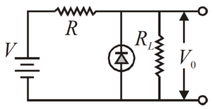
USE OF ZENER DIODE
For controlling voltage across tiny loads, the Zener diode is employed as a shunt voltage regulator. The voltage across the load will be stabilized by connecting the Zener diode in parallel to the load resistance RL.
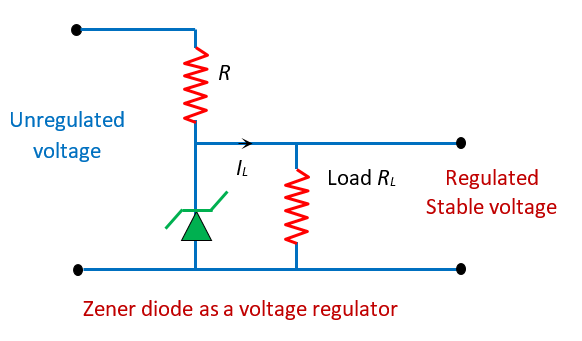
As discussed earlier that in reverse biasing when the applied voltage across the Zener diode surpasses the knee voltage, the Zener diodes have a stable breakdown voltage across a broad current range. We know that in parallel the voltage remains same therefore the load resistance gets the stable voltage of Zener diode.
PHOTO-DIODE
A photo-diode is a semi-conductor p-n junction diode. It is sensitive to light. In this diode light passes through a window onto the p-n junction. The arrows indicates the direction of incoming light. Figure given above shows the circuit of a photodiode. The photo-diode conducts in the reverse bias.
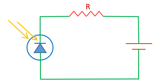
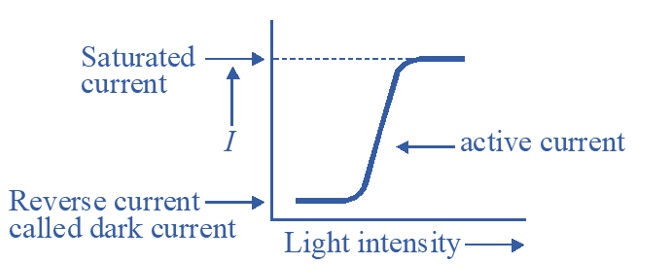
When no light is allowed to fall the diode acts as a normal reverse biased p-n junction diode, hence no current passes through it.When a light energy bombards a p-n junction, it dislodge valance electrons. The light produces free electrons and holes. The stronger the intensity of light , the greater the number of minority carriers and larger the reverse current as shown in the graph given below.
Light-emmitting diode (LED)
The LED is a semiconductor electronics device which radiates light when used in forward biasing. The basic principle behind this is the recombination of electrons and holes in a p-n junction diode.
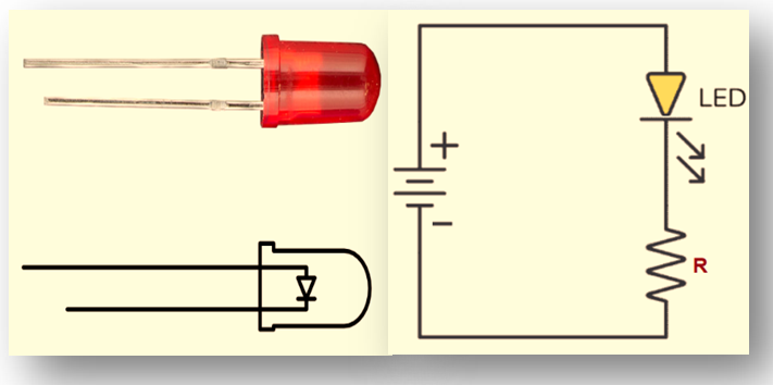
We know that the free electrons lies in conduction band at higher energy state whereas the holes exists in valance band in lower energy state. So as the conduction electrons move from higher energy level i.e. conduction band to lower energy level i.e. in holes which lies in valance band they radiate their excess energy. In an ordinary p-n junction diode energy radiated goes in the air in the form of heat. But in a LED, the energy is radiated as light. LED’s are made of gallium, arsenic or phosphorus material. They can radiate red, yellow, green, blue or orange light.. Figure given above shows how a LED actually looks like. On the right hand side of the diagram the circuit is given that shows the forward biased p-n junction diode (LED). LED’s are used in instruments like calculators and digital display. LED also find applications in burglar alarm systems. LED’s have replaced small indicator lamps. They operate on low voltage. They have a fast on-off switching and long life.
JUNCTION DIODE AS A RECTIFIER
Rectification is the process in which an ac signal is converted into a pulsating voltage that can vary in magnitude but does not reverse its direction. The simplest way to have rectification is to “cutt-off” one half of the input a.c. signal. The working principle is based on the fact that a diode has unidirectional flow of current, This happens because the resistance of a diode in forward biasing is very much lower as compared to the resistance in the reverse bias. Hence the diode conducts only in forward biasing i.e. if p region is at higher potential with respect to the n region. This property of diode has been used to restrict the voltage variation of ac to one direction only, and the phenomenon is known as rectification.
There are two types of rectifiers:
- Half wave rectifier
- Full wave rectifier
Half wave rectifier
Figure shown below gives the simplest rectifier circuit using a junction diode. This is known as a half-wave rectifier.. The input signal is applied to a the diodes D via a transformer. The diode is connected in series to a resistance \displaystyle {{R}_{L}}, known as load resistance.
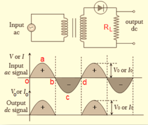
During the positive half cycle oab of the input signal let the current flows clockwise in the diode circuit as a result p region becomes positive with respect to the n region, hence the diode is forward biased and offer negligible resistance and therefore a current i flows in the circuit.
This current i produces a voltage drop across load resistance RL. As input signal increases or decreases the current i increases or decreases and so does the voltage drop across RL. The voltage drop across RL is the Output signal.
The variation of output voltage Vo during positive half cycle of input is shown in the output curve. During the negative half cycle, bcd of input signal, the current reverses its direction making p region as negative with respect to cathode and hence the diode becomes reversed biased and offer a very high resistance (theoretically infinite) making current i as zero and so is the output voltage. This is shown in output curve as a missing part. Since there is a output voltage only during the positive half cycle of input, the arrangement is known as half-wave rectifier. Obviously, efficiency of half-wave rectifier is even less than 50% It is found experimentally that Vo (dc) in a half wave rectifier is about 31.8% of the maximum value of the input a.c.
Various Parameters of half wave rectifier
(i) Output dc power
{{P}_{{dc}}}={{\left( {\frac{{{{I}_{0}}}}{\pi }} \right)}^{2}}{{R}_{L}}
(ii) Efficiency
Rectifier efficiency, \text{ }\!\!\eta\!\!\text{ }=\frac{{\text{Qutput dc power}}}{{\text{Input ac power}}} =\frac{{0.406}}{{1+\frac{{{{r}_{f}}}}{{{{R}_{L}}}}}}.
(iii) Ripple factor
\frac{{\text{rms}\text{. value of ac component}}}{{\text{value of dc component}}}=\frac{{{{I}_{{ac}}}}}{{{{I}_{{dc}}}}}=1.21.
Full Wave Rectifier
A full wave rectifier uses two diodes connected as shown in the figure given below. ABC is a center-tap transformer. The aim of the circuit is to pass a unidirectional current in the load resistance through the two diodes one by one .
To understand working of a full’ wave rectifier let us consider the positive half oab of the input cycle. Let point A of transformer be positive during this half of the input cycle. i.e. point A is at higher potential with respect to B. Hence the p region of diode D1 is positive with respect to its n region therefore it is forward biased and so it conduct the current through it. The direction of current flow is shown by solid arrow in the upper part of circuit. As point B is at a higher potential with respect to C. The diode D2 is reverse biased and consequently does not conduct. Therefore the current flows through the load resistance through diode D1.
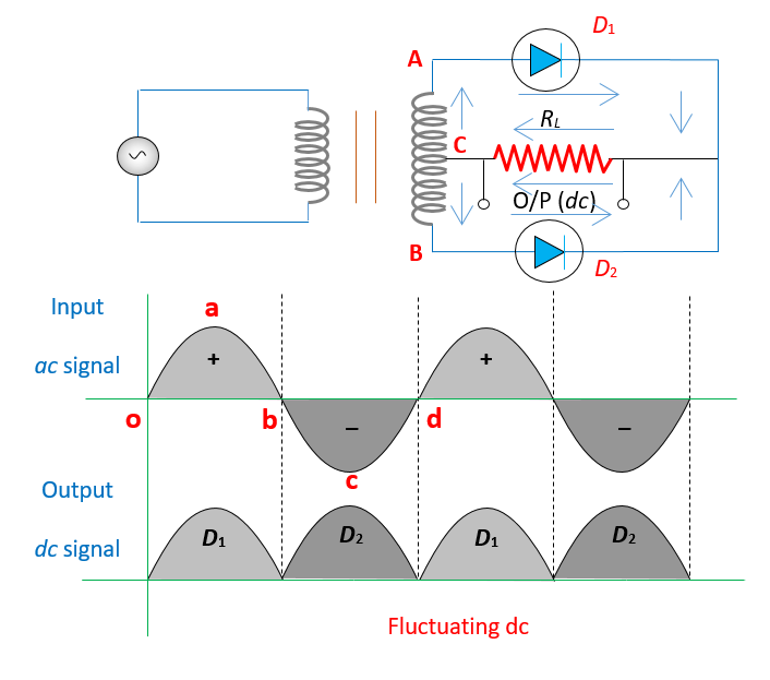
During the negative half bcd of the input cycle point. C is at a higher potential with respect to A. Obviously diode \displaystyle {{D}_{2}} is now forward biased and conduct the current through it. The direction of current is shown by solid arrows in the lower part of the circuit. The diode \displaystyle {{D}_{1}}, now is reverse biased and, therefore, does not conduct.
‘It. is clear from the circuit that direction of current through load, RL during both halves of the input signal is the same. And is from right to left in the load resistance according to the circuit diagram. The output voltage \displaystyle {{V}_{o}} varies as shown in the graphs of the input and output currents. Since there is an output during both halves of the. input signal, efficiency of a full-waves rectifier is nearly double that if a half-wave rectifier. In a full wave rectifier Vo (dc) is 63.7% of the maximum value of the ac applied.
Various parameters of full-wave rectifier
(i) Output dc power
Output dc power, \displaystyle {{P}_{{dc}}}={{I}^{2}}_{{dc}}.{{R}_{L}}
{{R}_{L}}={{\left( {\frac{{2{{I}_{0}}}}{\pi }} \right)}^{2}}{{R}_{L}}
(ii) Efficiency
Rectifier efficiency, \text{ }\!\!\eta\!\!\text{ }=\frac{{\text{Output dc power}}}{{\text{Input ac power}}} =\frac{{0.812}}{{\frac{{{{r}_{f}}}}{{{{R}_{L}}}}+1}}.
(iii) Ripple factor
=\frac{{\text{rms value of ac component}}}{{\text{value of dc component}}}=0.48.
BRIDGE RECTIFIER
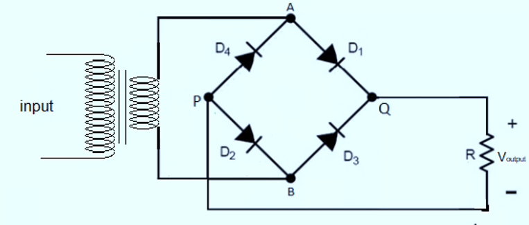
It is a most widely used full-wave rectifier. It uses four diodes. There is no need of centre tap secondary transformer. The circuit is given in the above diagram.
A.C. mains is applied through simple transformer or A.C. can be applied directly to rectifier. Full secondary voltage is applied to two diodes in series. During the positive half-cycle two diodes \displaystyle {{D}_{1}} and \displaystyle {{D}_{2}} becomes forward biased so current flows through these diodes, load resistance and back to secondary of transformer as shown in figure (a) given below
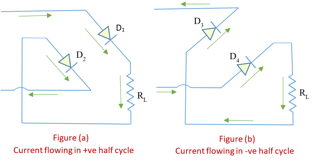
During the negative half cycle reverse happens, diodes \displaystyle {{D}_{3}} and \displaystyle {{D}_{4}} becomes forward biased and \displaystyle {{D}_{1}},{{D}_{2}}, reverse biased. Figure (b) shows current flow during negative half cycle. It is noted from the circuit that current always flow in load resistance in same direction during positive and negative half cycle.
Bridge rectifier circuit has the advantage that it does not require centre-tapped secondary winding transformer. It require small and less costly transformer. The main drawback of a bridge rectifier is that it requires four diodes. This circuit is not suitable for very low voltages. If step-down or step-up mains supply is not required the bridge rectifier can be used directly across the mains supply. The circuit becomes cheaper and there is no need for the transformer.
Illustration
A p-n junction diode cannot be used
(1) as a rectifier
(2) for getting light radiation
(3) for converting light energy into electrical energy
(4) as an amplifier.
Solution
A p-n junction diode cannot be used as an amplified.
Hence correct option is (4)
Illustration
When a p-n junction is forward biased, the flow of current across the junction is mainly due to
(1) drift of charges
(2) diffusion of charges
(3) both drift and diffusion of charges
(4) depends on the nature of the material.
Solution
When a p-n junction is forward biased, the flow of current across the junction is mainly due to diffusion of charge.
Hence correct option is (2)
Illustration
Zener diodes are used for
(1) rectification
(2) amplification
(3) stabilization of voltage
(4) production of carrier waves.
Solution
Zener diodes are used for stabilization of voltage
Hence correct option is (3)
Illustration
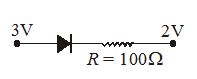
The diode used in the circuit shown in figure has a constant voltage drop at 0.6 V at all currents and a maximum power rating of 150 mW. Find the value of R for obtaining maximum power.
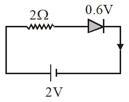
Solution
Diode resistance, {{R}_{d}}=\frac{{V_{d}^{2}}}{P}=\frac{{0.6\times 0.6}}{{0.150}}=2.4\text{ohm,}
where Vd is potential drop across the diode.
Current through diode, {{I}_{d}}=\frac{{{{V}_{d}}}}{{{{R}_{d}}}}=\frac{{0.6}}{{2.4}}=0.25\text{A}
Total resistance in the circuit, {{R}_{f}}=\frac{V}{{{{I}_{d}}}}=\frac{2}{{0.25}}=8\text{ohm}
Therefore R=8-2.4=5.6\,\text{ohm}\text{.}
Illustration
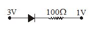
The circuit shown in the figure contains two diodes each with a forward resistance of 50 ohm and with infinite reverse resistance. If the battery voltage is 6V, find the current through the 100 ohm resistance.
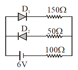
Solution
As per given circuit, diode \displaystyle {{D}_{1}} is forward biased and offer a resistance of 50 ohm. Diode \displaystyle {{D}_{2}} is reverse biased as a its corresponding resistance in infinite, no current flows through it. Thus the branch containing {{D}_{2}} can be removed . Hence the circuit contains three resistance of {{D}_{1}}, 150 \ohm and 100 \ohm in series.
As all the three resistances are series, so the current through them is
I=\frac{{6V}}{{50+150+100}}\text{ohm}=\frac{6}{{300}}\text{A}=0.02\text{A}
Illustration
Assume that the supply voltage V is 10 volt and the Zener voltage \displaystyle {{V}_{o}} is 6.5 volt. If the maximum Zener current be 22 mA, determine the series resistance R and load current when the load resistance is 1 \mathbf{K}\Omega .
Solution
Zener current is maximum when load resistance \displaystyle {{R}_{L}} is infinite.
R=\frac{{V-{{V}_{0}}}}{I}=\frac{{10-6.5}}{{22\times {{{10}}^{{-3}}}}}=159\,\,\text{ohm}.
The current through the load resistance,
Given RL = 1k\Omega .
{{I}_{L}}=\frac{{{{V}_{0}}}}{{{{R}_{L}}}}=\frac{{6.5}}{{{{{10}}^{3}}}}A=6.5\text{mA}
Illustration
A semi conductor X is made by doping a germinium crystal with arsenic (Z=33). A second semi conductor Y is made by doping germinium with indium (Z=49). The two are joined end to end and connected to a battery as shown.
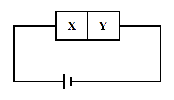
Which of the following statements is correct?
(1) X is p-type, Y is n-type and the junction is forward biased
(2) X is n-type, Y is n-type and the junction is forward biased
(3) X is p-type, Y is n-type and the junction is forward biased
(4) X is n-type, Y is p-type and the junction is reversed biased.
Solution
Arsenic is pentavalent and is a donor impurity and supplies extra electrons, so electrons become majority change carriers and the material becomes n-type where as indium is trivalent and is an acceptor impurity and supplies holes, which become majority charge carriers and the material behaves as p-type semi conductors.
Illustration
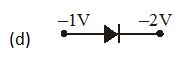
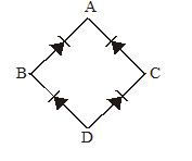
In the network shown choose the correct option
(1) the potential difference across \displaystyle {{D}_{2}} is 5V
(2) current through resistor equals 1.25 A
(3) current through diode \displaystyle {{D}_{1}} is 1.25 A
(4) current through diode \displaystyle {{D}_{2}} is 1.25 A
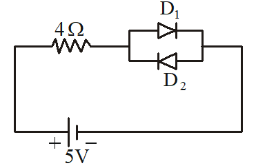
Solution
In the given circuit diode \displaystyle {{D}_{1}} is forward biased and \displaystyle {{D}_{2}} offers infinite resistance.
Current through resistors and \displaystyle {{D}_{1}} is \frac{5}{4}=1.25 A.
Hence correct option are (2) & (3)
Illustration
A sinusoidal voltage of rms value of 200 volt is connected to the diode and capacitor C is the circuit shown so that half wave rectification occurs. The final potential difference is volt across C is
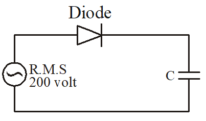
(1) 500
(2) 200
(3) 283
(4) 141
Solution
When the n-p-junction is forward biased, the capacitor is charged to the peak voltage of sinusoidal voltage which is the maximum voltage reached across capacitor.
hence maximum voltage reached is = {{E}_{0}}={{E}_{{rms}}}\times \sqrt{2} = 200\sqrt{2}=283\,V
Hence correct option is (3)
Illustration
In a p–n junction diode when forward biased has a drop of 0.5V which is assumed to be independent of current. The current of 10mA through the diode produces a large Joule heat which damages (burns) the diode. If we want to use a 1.5 V battery to forward bias the diode, what should be the value of resistor used in series with the diode so that the maximum current does not exceed 5mA?
Solution
The value of R should be such that the current in the circuit does not exceed 5 mA.
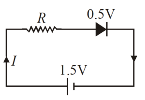
By KVL we have
I\times R+0.5\text{V}=1.5\text{V}
or 5\times {{10}^{{-3}}}\times R=1.0\text{V}
or R=200\Omega .
Illustration
A battery of 2V may be connected across the points A and B, as shown in figure. Find the current drawn from the battery if the positive terminal is connected to (i) the point A and (ii) the point B. Assume that the resistance of each diode is zero in forward bias and infinity in reverse bias.
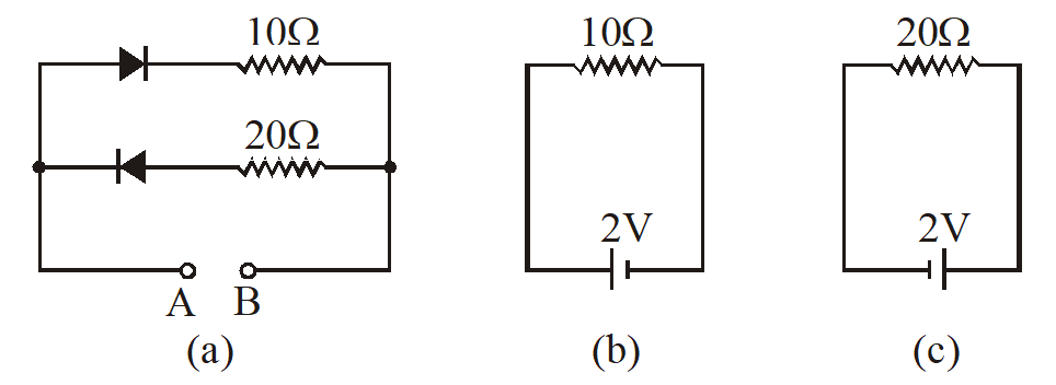
Solution
(a) When positive terminal of the battery is connected to point A, diode \displaystyle {{D}_{1}} gets forward biased and offers zero resistance and diode \displaystyle {{D}_{2}} gets reverse biased and offers infinite resistance. The given circuit reduces to the equivalent circuit shown in figure (b).
Hence current drawn from the battery, I=\frac{2}{{10}}=0.2\text{A}.
(b) When positive terminal of the battery is connected to point B, the diode \displaystyle {{D}_{2}} gets reverse biased and offers infinite resistance and diode \displaystyle {{D}_{2}} gets forward biased and offers zero resistance. The given circuit reduces to the equivalent circuit shown in figure (c).
Therefore current drawn from the battery, I=\frac{2}{{20}}=0.1\text{A}.
Practice Questions (Basic Level)
1.
A semiconductor has the electron concentration 0.45 × 10¹² m–3 and hole concentration 5 × 10²⁰ m–3. Find its conductivity. Given: electron mobility = 0.135 m2V–1s–1 and hole mobility = 0.048 m2v–1s–1; e = 1.6 × 10⁻¹⁹ coulomb.
(a) 1.548 \displaystyle \Omega m–1
(b) 1.224 \displaystyle \Omega m–1
(c) 3.845 \displaystyle \Omega m–1
(d) 0.456 \displaystyle \Omega m–1
Ans (c)
2.
When the voltage drop across a p–n junction diode is increased from 0.70V to 0.71 V, the change in the diode current is 10 mA. What is the dynamic resistance of the hole?
(a) 27 \displaystyle \Omega
(b) 20 \displaystyle \Omega
(c) 4 \displaystyle \Omega
(d) 1 \displaystyle \Omega
Ans (d)
3.
In a p type semiconductor the acceptor level is situated 57 meV above the valence band. The maximum wavelength of light required to produce a hole will be
(a) 57 × 10–3Å
(b) 11.61 × 10⁻³³ watt
(c) 57 Å
(d) 217100 Å.
Ans (d)
4.
The band of maximum energy in which electrons are present is called
(a) valence band
(b) forbidden band
(c) conduction band
(d) fermi band.
Ans (a)
5.
The relation between the number of free electrons in semiconductors (n) and its temperature (T) is
(a) n \displaystyle \propto T
(b) n\propto \sqrt{T}
(c) n \displaystyle \propto T3/2
(d) n \displaystyle \propto T2.
Ans (c)
6.
The electron mobility in an n type germanium is 3900 cm2/V-s and its conductivity is 6.24 mho cm–1, then the impurity concentration will be
(a) 1016/cm3
(b) 1015/cm3
(c) 1013/cm
(d) 1012/cm3.
Ans (a)
7.
Polymers are the substance which are
(a) amorphous in nature
(b) semi-solids
(c) crystalline in nature
(d) none of these.
Ans (d)
8.
In which case is the junction diode forward biased

Ans (d)
9.
Acceptor type or p type semiconductor is formed by adding impurity of valency
(a) 6
(b) 5
(c) 4
(d) 3.
Ans(d)
10.
The ripple factor in a full-wave rectifier is
(1) 0.48
(2) 1.21
(3) 0.62
(4) 1.0.
Ans (a)
11.
Assuming that the junction diode is ideal, the current in arrangement as shown in figure is
(a) 2 mA
(b) 10 mA
(c) 20 mA
(d) 30 mA.
Ans (b)
Practice Questions (JEE Main Level)
1.
The number density of electrons and holes in intrinsic silicon at a given temperature is 4.94 × 1010 cm–3. Calculate the resistivity and conductivity of the silicon. Given electron mobility = 100 cm2V–1s–1 and hole mobility –1000 cm2 V–1 s–1.
(a) 9 × 10⁴ \displaystyle \Omega cm, 0.5 × 10⁻⁶ s cm–1
(b) 9 × 10⁴ \displaystyle \Omega cm, 11.1 × 10⁻⁶ s cm–1
(c) 2 × 10⁴ \displaystyle \Omega cm, 10.4 × 10⁻⁶ s cm–1
(d) 9 × 10⁴ \displaystyle \Omega cm, 7.15 × 10⁻⁶ s cm–1
Ans (b)
2.
Determine the number density of donor atoms which have to be added to an intrinsic germanium to produce an n-type semiconductor of conductivity 0.06 sm–1. Given the mobility of electrons = 0.39 m2v–1s–1. Neglect the contribution of the diode?
(a) 87 × 1016 m–3
(b) 34 × 1016 m–3
(c) 0.45 × 10¹⁶ m–3
(d) 96 × 1016 m–3
Ans (d)
3.
A p–n junction is designed to withstand currents upto a maximum current of 10 mA. A resistance of 200W is connected in series with it. When forward biased, the diode has a potential drop of 0.5V which is assumed to be independent of current. Find the maximum voltage of the battery to forward bias the diode.
(a) 1.4V
(b) 9.2V
(c) 2.5V
(d) 3.4V
Ans (c)
4.
The safe limits of temperature for germanium and silicon care
(a) 8 × 10² °C and 2 × 10² °C
(b) 80°C and 2 × 10² °C
(c) 2 × 10³ °C and 80°C
(d) 2 × 10² °C and 800°C.
Ans (b)
5.
The potential barrier of silicon at 30° C is 0.7 eV, then its value at 13° C will be
(a) 0.9 eV
(b) 0.6 eV
(c) 0.67 eV
(d) 0.7 eV.
Ans (c)
6.
A solid which is not transparent to visible light and shoes electrical conductivity decreases with temperature is formed by
(a) ionic bonding
(b) van der wall bonding
(c) metallic bonding
(d) covalent bonding.
Ans (c)
7.
In the arrangement shows in figure below, the current through diode is
(a) 1 mA
(b) 10 mA
(c) 20 mA
(d) zero.
Ans (c)
8.
On doping germanium with donor atoms of density 1017 cm–3, its conductivity in mho cm–1 will be —— if m = 3800 cm2/V-s and ni = 2.5 × 1013 cm–3
(a) 240
(b) 180
(c) 120
(d) 60.8
Ans (c)
9.
The number of densities of electrons and holes in pure silicon at 27°C are equal and its value is 1.5 × 10¹⁶ m–3. On doping with indium, the hole density increases to 4.5 × 10²² m–3. The electron density in doped silicon will be
(a) 108 m–3
(b) 107 m–3
(c) 50 × 109 m–3
(d) 5 × 10⁹ m–3.
Ans (c)
10.
A silicon specimen is made into a p type semiconductor by doping, on an average one indium atom per 5 × 10⁷ silicon atom. If the number density of atom in the silicon specimen is 5 × 1028 atom/m3 then the number of acceptor atoms in silicon per cm3 will be
(a) 1.0 × 10¹⁵
(b) 2.5 × 1036
(c) 2.5 × 1030
(d) 1.0 × 10³.
Ans (d)
11.
Two identical p-n junction may be connected in series with a battery in three ways as shown in figure. The potential drop across the p–n junction are equal in
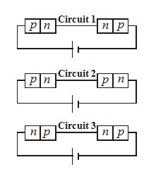
(a) circuit 3 and circuit 1
(b) circuit 1 and circuit 2
(c) circuit 2 and circuit 3
(d) only circuit 1.
Ans (c)
12.
For the given circuit shown is figure, to act as full-wave rectifier, the ac input should be connected across … and then dc output would appear across …
(a) A B, C D
(b) A C, B D
(c) B C, A D
(d) B D, A C.
Ans (d)
Practice Questions (JEE Advance Level)
Lorem ipsum dolor sit amet, consectetur adipiscing elit. Ut elit tellus, luctus nec ullamcorper mattis, pulvinar dapibus leo.