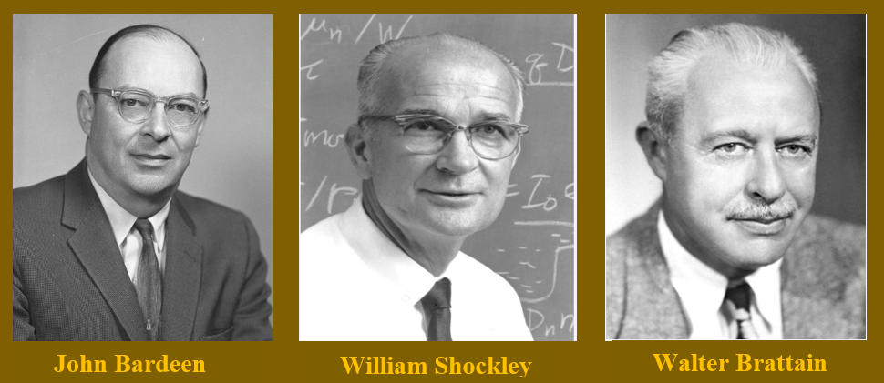
In 1956 three American scientists shared the Nobel prize for their research on semiconductors and their discovery of the point contact transistor . They were, William Bradford Shockley and Walter Houser Brattain. Bardeen was a quantum physicist, Shockley was an expert in solid state physics and Brattain was a gifted experimenter in material science
John Bardeen was an American electrical engineer and scientist who was born on May 23, 1908. He is the only person to have received the Nobel Prize in Physics twice. First for discovery of transistor and second for BCS theory, a fundamental theory of conventional superconductivity.
William Bradford Shockley Jr. was an American inventor, physicist born on February 13, 1910. He oversaw the research team at Bell Labs. Shockley’s efforts to commercialize a novel transistor design in the 1950s and 1960s contributed to Silicon Valley’s rise as a centre of electronics innovation in California.
Born on February 10, 1902, Walter Houser Brattain was an American physicist who worked at Bell Labs. The photo-effect at a semiconductor’s free surface was discovered by Brattain. The Nobel Prize committee regarded this work as one of his most important contributions to solid state physics.
Introduction Of Chapter
Prior to the 1948 discovery of the transistor, the main components used in the electronic circuits were primarily the vacuum tubes, also known as valves. Examples of these include the vacuum diode, which has two electrodes: the cathode and the anode (sometimes referred to as the plate); the triode, which has three electrodes: the cathode, plate and grid; and the tetrode and pentode, which have four and five electrodes, respectively. These vacuum tube devices are large in size , consumes more power , typically run at high voltages (100 V), have a short lifespan, and are not very reliable.
The discovery that certain solid-state semiconductors and their junctions give the ability to control the quantity and direction of charge carrier flow across them in the 1930s served as the foundation for the creation of today’s solid-state semiconductor electronic devises like p-n junction diodes and transistors etc.
One can alter the amount of mobile charges in a semiconductor by applying a tiny voltage, applying light, or both. Observe that in semiconductor devices, the supply and flow of charge carriers occur within the solid, whereas in previous vacuum tubes and valves, the mobile electrons were derived from a heated cathode and they were made to flow in an evacuated space or vacuum. No external heating or large evacuated space is required by the semiconductor devices. They are small in size, consume low power, operate at low voltages and have long life and high reliability. Even the Cathode Ray Tubes (CRT) used in television and computer monitors which work on the principle of vacuum tubes are being replaced by Liquid Crystal Display (LCD) monitors with supporting solid state electronics.
The fundamental ideas of semiconductor physics will be covered in this chapter, along with a discussion of several semiconductor devices, such as bipolar junction transistors (a 3-electrode device) and junction diodes (a 2-electrode device). Also there will also be descriptions of a few circuits that show how they are used.